//www.oemsecrets.com/compare/%20ESP32-C61-DevKitC-1-N8R2 ### Digilent Analog Discovery Studio Max - Labor in der Schuhschachtel Wer eine Steckplatine hat, hat drumherum normalerweise verschiedenste Unterstützungshardware. Im Hause Digilent möchte man nun mit dem in der Abbildung gezeigten und
to 10,000, and using bipolar process. Characteristics such as low input offset voltage (125 μV max.), Low input offset voltage drift (1 μV/°C max.), High CMR (110 dB min. at G = 100), and low input bias current (2 nA max.) I [/c] ### Infineon CCG7SCF - USB-PD-Controllerschaltkreis. Bauteile
I2C_HSM_EN=0 I2C_HSM_EN=1 (FastMode) (HighSpeedMode) TestConditions/ Parameter Symbol Comments Min Max Min Max Unit DCINPUTLEVELS InputVoltage LowLevel V 0.3×V 0.3×V V IL DDIO DDIO HighLevel VIH 0.7×VDDIO 0.7×V DDIO V HysteresisofSchmittTriggerV 0.05×V 0.1×V V HYS DDIO DDIO Inputs InputCurrent IL 0.1
Windungszahl sinken die Verluste der mehr- lagigen Wicklung im Verhältnis zur einlagigen Wicklung ab und das Max. Duty Cycle 0.8 Verlust-Verhältnis erreicht z.B. für N1= 10 den Wert 0.34. Ausgangsinduktivität 30µH Zu beachten ist, dass mit der steigenden Lagenzahl das Volumen der Wicklung sowie die parasitäre
channel 6 N7 Close channel 7 N8 Close channel 8 N9 Close channel 9 N10 Close channel 10 N11 Step mode, max channel is 2 N13 Step mode, max channel is 4 N14 Step mode, max channel is 5 N15 Step mode, max channel is 6 N16 Step mode, max channel is 7 N17 Step mode, max channel is 8 N18 Step mode, max channel is 9 N19 Step mode, max channel is 10 N20 Open all - stop scanning or stepping if applicable Scanning (cont.) N21 Scan mode, max channel is 2 N22 Scan mode, max channel is 3 N23 Scan mode, max channel is 4 N24 Scan mode, max
: 74h Size: 8 bits Table 3-213 Lock Count Bit Access Symbol Description [7:4] R/W locked_cnt_noisy_max These bits set the max value of the hlock sensor for noisy signals. 8 is added to this value. Default = 7 stands for 15. These bits set the max value of the hlock sensor for clean signals. 8 is [3:0] R/W locked_cnt_clean_max added to this value. Default = 4 stands for 12. 3.9.18 H Loop Max State Address Offset: 17h Access: Read/Write Default Value: CBh Size: 8 bits 83 电子专业技术主页: HTTP://WWW.LCDHOME.NET 资料收藏: 版权归原作者所有 谨供学习用
Max schrieb im Beitrag #7907261: > > Der Mosfet muss wie die SBR im Bereich 100V oder mehr dimensioniert > sein, die Schaltung dahinter ist ein Spannungsregler der max 40V > verträgt und max 1,3A
Hallo Max, Max schrieb im Beitrag #7907261: > Nun möchte ich einen großen Elko verwenden um diese Monster zu bändigen. > Das Problem ist nur dass der Einschaltstrom eines entsprechenden Elkos > zu gross
= 3/8” PD 500 mW Fax: (978) 689-0803 Working Peak Voltage VWM 100 V Solder Pad Temperature @ 10 s max. T 260 oC SP MSC – Ireland o Gort Road Business Park, Notes: 1. Derate at 4mW/°C above +50 C. Ennis, Co. Clare, Ireland Tel: +353 (0) 65 6840044 Fax: +353 (0) 65 6822298 Website: www.microsemi.com T4
commonmodeconfiguration FB20010-3B-RC 21/2 520 780 B FB20020-4B-RC 21/2 30 330 B • Operating/storagetemperature:-40to+105°C FB20011-3B-RC 2x11/2 265 430 C • Ratedcurrent:5Awith20°Cmax.temperaturerise FB20021-4B-RC 2x11/2 160 460 C FB20022-4B-RC 3 640 900 D *RoHSDirective2015/863,Mar31,2015andAnnex. “-RC”su xindicatesRoHScompliance. 0.138 0.236 45° 0.394 Core Dimension 0.024 0.55 Max. 1.5 Fig. A Fig. B Fig. C Fig. D Dimensions: Inches WARNING Cancer and Reproductive Harm www.P65Warnings.ca.gov Specifications are subject to change without notice. Users should verify actual device
Systeme über den Jordan zu treiben. MaxLinear schickt nun eine Serie von Empfängerbausteinen ins Rennen, die – wie in der Abbildung gezeigt – RS485 und RS-422 verarbeiten können. Die maximale Datenrate liegt dabei im Bereich 65Mbps.  Bildquelle: MaxLinear Über die Robustheit vermeldet das Datenblatt folgendes: [c] ±4kV EFT (IEC 61000-4-4) ±12kV ESD Contact (IEC 61000-4-2) ±15kV ESD Human Body Model [/c] ### Melexis MLX90642
IS UNCONTROLLED IN P AND P BEYOND DIMENSION K MINIMUM. L SEATING INCHES MILLIMETERS PLANE K DIM MIN MAX MIN MAX A 0.175 0.205 4.45 5.20 B 0.170 0.210 4.32 5.33 C 0.125 0.165 3.18 4.19 D 0.016 0.021 0.407 0.533 X X D G 0.045 0.055 1.15 1.39 G H 0.095 0.105 2.42 2.66 J 0.015 0.020 0.39 0.50 H J K 0.500 --- 12.70 --- L 0.250 --- 6.35 --- V C N 0.080 0.105 2.04 2.66 P --- 0.100 --- 2.54 SECTION X−X R 0.115 --- 2.93 --- 1 N V 0.135 --- 3.43 --- N A BENT LEAD NOTES: R B 1. DIMENSIONING AND TOLERANCING PER TAPE & REEL ASME Y14.5M, 1994. AMMO PACK 2. CONTROLLING
3.3V Power Supplies with 48kHz input data) unless otherwise noted. PARAMETER TEST CONDITIONS MIN NOM MAX UNIT Dynamic range TAS5558 A-weighted (Test Range: 20Hz to 20kHz. fS= 105 dB 96 kHz). Total harmonic distortion TAS5558 output (1kHz at -1dBFS) 0.01% 32-kHz to 96-kHz sample rates (Test Range 20Hz -
temperature Component: –40°C to +165°C. Tape and reel packaging: –40°C to +80°C Resistance to soldering heat Max three 40 second reflows at +260°C, parts cooled to room temperature between cycles Moisture Sensitivity Level (MSL) 1 (unlimited floor life at <30°C / 85% relative humidity) Recommended pick and place
as those used on the adapter board included with the kit. The part number for this header is: FTSH-105-01-L-DV-K-A-P from SAMTEC. Atmel Atmel-ICE [USER GUIDE] 52 Atmel-42330C-Atmel-ICE_User Guide-10/2016 6. Software Integration 6.1. Atmel Studio 6.1.1. Software Integration in Atmel Studio Atmel Studio
Verlustleistung) und die Lebensdauer. Daher lasse ich auf Layouts immer möglichst viel Kupfer (evtl. 70 oder 105er Dicke) stehen, weil es die Wärme gleichmäßig verteilt. Die 3 Dioden sind ein Kompromis, dadurch wird die Wärme reduziert (niedrigere Flußspannung) und besser verteilt. Nachteile sind der Preis, Fläche
allein dem Aufladen eines Smartphones > problemlos funktionierte, was - gemessen - einen Strom von max. ca. > 900mA bedeute (das Ladegerät ist "dumm", stellt den Strom nicht nach > Bedarf, D+ und D- sind über einen niederohmigen Spannungsteiler von > addiert ca. 150R mit Masse und +5V verbunden
pulses per minute maximum. ELECTRICAL CHARACTERISTICS (TA= 25°C unless otherwise noted, F = 3.5 V Max. @ F (Note 4) = 30 A, F = 1.3 V Max. @ F (Note 4) = 3 A) (Note 5) I Symbol Parameter F PP Maximum Reverse Peak Pulse Current VC Clamping Voltage @ PP V RWM Working Peak Reverse Voltage V V V IR Maximum
differentially drive an air–core meter. ORDERING INFORMATION IL8190N Plastic DIP IL8190DW SOIC TA= -40 to 105 C ORDERING INFORMATION Operating Temperature FEATURES Device Range Package Packing IL8190N DIP-16 Tube IL8190DW T = -40 to 105 C SOP-20 Tube Direct Sensor Input A High Output Torque IL8190DWT
Table 19-6 Low-speed oscillator (LSI and LSE) Symbol Parameter description Min. Typ. Max. Unit FLSIR Internal LSI oscillator frequency 24 42 KHz T SULSIExternal LSE oscillator startup to stabilization time 40 100 uS Table 19-7 PLLcharacteristics Symbol Parameter description Min. Typ. Max
Figure 2 Minimum Fan Speed Requirements: Start Pulse Startup Pulse - Speed vs. Time %of full speed 35 Max % of full speed 30 RPM for startup 25 Max duration of startup pulse 20 15 10 5 0 0 0.5 1 1.5 2 2.5 3 Time (seconds) 13 Fan Speed Control 3.3 Fan Speed Response to PWM Control Input Signal The PWM input
range -40 to 150 °C Recommended max. power dissipation @TA= 70 °C (DIP16) 1 P TOT W Recommended max. power dissipation @TA= 50 °C (SO16) 0.83 7/36 Electrical characteristics L6599 5 Electrical characteristics T J 0 to 105 °C, V CC = 15
from 0°C to +125°C, unless otherwise specified; For NCP1605DR2G: for typical valuesJT = 25°C, for min/max valJes T = −55°C to +125°C, unless otherwise specified) (Note 7) Symbol Rating Min Typ Max Unit Gate Drive Section Trise Output Voltage Rise Time @LC = 1 nF, from 1 V to 10 V − 40 − ns T fall Output
Figure 1 Minimum Fan Speed Requirements: Start Pulse Startup Pulse - Speed vs. Time %of full speed 35 Max % of full speed 30 RPM for startup 25 Max duration of startup pulse 20 15 10 5 0 0 0.5 1 1.5 2 2.5 3 Time (seconds) 11 Fan Speed Control 3.3 Fan Speed Response to PWM Control Input Signal The PWM input
14.4 V • P o 4 (25 W / 10) = 4 2.5 W into 4 (audio with crest factor of 10) • T = 25 C amb • P max = 4 W (from Figure 24) • R th(j-a) 12 K/W • Tj(max) = 25 C + (4 W 12 K/W) = 73 C 14.5 Curves measured in reference design 102 aaa-000451 102 aaa-000452 THD + N THD + N (%) (%) 10 10 1 1 (1) (1)
temperature, R ILIM= 400 Ω, unless otherwise noted. TPS2112A TPS2113A PARAMETER TEST CONDITIONS MIN TYP MAX MIN TYP MAX UNIT VI(IN1)VI(IN2)5.0 V 120 140 84 110 T J 25°C, IL= 500 mA VI(IN1)VI(IN2)3.3 V 120 140 84 110 mΩ Drain-source V = V = 2.8 V 120 140 84 110 on-state rDS(on)) I(IN1) I(IN2) resistance VI
°C 62 75 mΩ OUT = -200 mA -40°C to 85°C 90 mΩ ON-State Resistance (TPS2120) V > V PRI REF -40°C to 105°C 100 mΩ VINx≥ 5.0 V -40°C to 125°C 120 mΩ R ON 25°C 56 70 mΩ I = -200 mA OUT -40°C to 85°C 85 mΩ ON-State Resistance (TPS2121) VPRI> V REF VINx≥ 5.0 V -40°C to 105°C 90 mΩ -40°C to 125°C 100 mΩ CURRENT
5.5 V, and RILIM 400 Ω, unless otherwise noted. TPS2114A TPS2115A PARAMETER TEST CONDITIONS MIN TYP MAX MIN TYP MAX UNIT T J 25°C, L = 500 mA, I(IN1)VI(IN2)5.0 V 120 140 84 110 mΩ T = 25°C, I = 500 mA, V = V = 3.3 V 120 140 84 110 mΩ J L I(IN1) I(IN2) Drain-source on-state T J 25°C, L = 500 mA, I(IN1)
deren Auswertung häufig für fertige Schaltkreise mit passendem Verstärker und A/D-Wandler, wie dem MAX31865. Im Interesse einer präzisen Funktion sollte dieser dennoch am besten mit einer vom Mikrocontroller entkoppelten stabilisierten Spannung betrieben werden. Serienwiderstände in den I2C-Leitungen
Devices besitzt eine Auflösung von 16 Bit und eine Genauigkeit von ±0.5°C im Bereich von −40°C bis +105°C. Vorteile: Ansteuerung per SPI ADT73xx oder I2C ADT74xx keine Kalibrierung notwendig hohe Auflösung und Genauigkeit: 16 Bit ADT7x02 2,00° ADT7x01 1,00° ADT7x10 0,40 / 0,50° ADT7x20 0,20 / 0,25° auch
so it can measure a wider temperature measurement range. Please note! the MAX31855 is not pin compatible or drop-in code compatible with the MAX6675. We do have an Arduino library for both chips but you'll need to adjust any existing MAX6675 designs for the mew MAX31855. The
kritischer Bauteile (z.B. ICs oder LEDs). Die Minimalbestückung sieht einen MAX6675/MAX31855 vor. Die Auswahl in der Firmware erfolgt über einen der beiden GPIO-Pins RA5 oder RA0 via dem ChipSelect (CS) des MAX6675/MAX31855. Neben dem MAX6675/MAX31855 wurde ein Decoupling-Kondensator
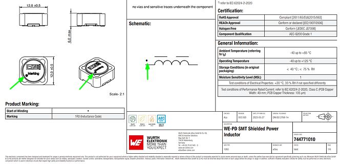
12,0 ±0,5
6,0 max.
12,0 ±0,5
Marking
Schematic:
no vias and sensitive traces underneath the component
1) refer to IEC 62024-2-2020
Certification:
RoHS Approval Compliant [2011/65/EU&2015/863]
REACH Approach Conform or
für den Betrieb ein Problem darstellt? Hat da jemand Erfahrung damit? Laut Datenblatt scheint eine max. Temperatur von 150 Grad akzeptabel. Viele Grüße Thomas, DL8TF
Tatsächlich sind in der Nähe Elkos verbaut. Die Temperaturen dort liegen bei ca. 50 - 60 Grad. Es sind 105 Grad Typen. Vermutlich wäre es besser diese weiter entfernt anzubringen. Viele Grüße Thomas
A .50 mA Hipot rating (one minute): Line to Ground: 2250 VDC Line to Line: 1450 VDC Rated Voltage(max.): 250VAC S Model Operating Voltages: LINE LOAD Selectable or Fixed 115/230 VAC Operating Frequency: 50/60 Hz Rated Current: Non-Filtered – 10A Filtered – 3, 6 or 10A L Model Fuseholder: Accepts one
105 ℃ Table 3-3 Power-on and power-down conditions Symbol Parameter Condition Min. Max. Unit VDD V DD rise time rate 0 ∞ us/V V DD fall time rate 30 ∞ 3.3.2 Embedded reset and power control block characteristics
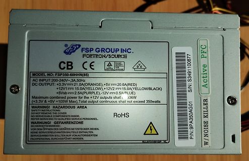
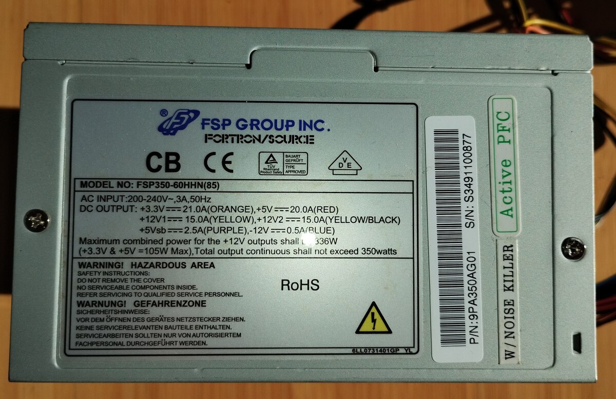
YELLOW/BLACK)
-12V==0.5A(BLUE)
Maximum combined power for the +12V outputs shall be 336W
(+3.3V & +5V=105W Max), Total output continuous shall not exceed 350watts
WARNING! HAZARDOUS AREA
SAFETY INSTRUCTIONS:
DO NOT REMOVE THE COVER
NO SERVICEABLE COMPONENTS INSIDE.
REFER SERVICE TO QUALIFIED SERVICE PERSONNEL
kann man nur mit dem Oszi messen, wenn es wieder > läuft. der Glättungselko dahinter hat auch nur max 25V - kann es einen Sinn haben hier Dioden mit so einer hohen maximalen Spannung einzubauen? Wolf17 schrieb im Beitrag #7876858: > Elkotausch ist nie verkehrt, wenn schon alles freiliegt. > Ist
sagt aber > nichts ob der ESR gut oder schlecht ist. ja genau Elkos habe ich da, wohl keine 105° Typen, aber ist der jetzige ja auch nicht
current loop interface a) Type of signal 20 mA current loop Absolute limits: Open-circuit voltage: max. 30 V d.c. Loop current: max. 30 mA Table 1 – Electrical interface Current Send (TX) Receive (RX) Zero, no loop current, SPACE ≤2,5 mA ≤3 mA One, 20 mA loop current, MARK ≥11 mA ≥9 mA Voltage drop Send
XP-Power. > > Danke Hinz, perfekter Hinweis!!! Naja, das Ding macht 250V bei 6A, kann angeblich auf 105% = 262V eingestellt werden. Da fehlen noch 18V bis 280V. Die 400V Version kann 3,75A.
> >> Danke Hinz, perfekter Hinweis!!! > > Naja, das Ding macht 250V bei 6A, kann angeblich auf 105% = 262V > eingestellt werden. Und weitere 5% am Trimmer. Macht also 275V, mindestens.
20 A1, Frequenz- Smart PLGS 2012 A1. leistung.......≤20dBm Frequenzband ..2400-2483,5MHz Temperatur.max 50 °C Ladevorgang 0 - 10 °C, bzw. 50 - 60 °C bei einem Ladestrom von max. 4 A 10 - 50 °C bei einem Ladestrom von max. 12 A Betrieb......-20 - 50 °C Lagerung 8 DE AT CH Ladezeit Akku Smart PAPS 208 A1
otherwise specified)(Note 1) For UTC LM7833 (V =5.8V) IN PARAMETER SYMBOL TEST CONDITIONS MIN TYP MAX UNIT T =25°C, I =5mA - 1.0A 3.168 3.30 3.432 V J OUT Output Voltage VOUT V IN.8V ~ 18.3V, I =5mA - 1.0A, P ≦15W 3.135 3.465 V OUT D Dropout Voltage VD T J25°C 2.0 V Load Regulation ΔV OUT T J25°C,I
This feature allows to save battery In/Out settings power. Overload [10 %] [15 %] [20 %] ... [100 %] [105 %] prealarm [105 %] Gives a warning when a predefined critical percentage of load is reached. Cold start [Disable] [Enable] Enable Enables the product to be started on battery power. First cold start
2.54 mm, we developed a x 0.63 mm pin contact and new automobile suitable reaches at this point a max. contact system. The positive load of current carrying capa- features of existing contact city of up to 7.5 A at 80 °C. systems – high packing density and at the same time Based on the plug uniform
Character size 3.20(W) × 5.55(H) mm Viewing area 83.0(W) × 18.5(H) mm Module size 116.0(W) ×37.0(H) × 10.0max (T) mm Module size mm 116.0(W) ×37.0(H) × 14.5max (T)) (w/ LED back-light) 4 ABSOLUTE MAXIMUM RATINGS Parameter Symbol Min Max Unit Logic Circuit Supply Voltage VDD-VSS -0.3 7.0 V LCD Driving Voltage

 Bild
 Bild