-
PDF
LCD-Controller_NT3881.pdf
1 100 AH RS, R/W Address Hold Time 10 - - ns Figure 1 RD Read Data Output Delay - - 190 ns Figure 1 tDHR Read Data Hold Time 20 - - ns Figure 1 8 V2.5 NT3881D AC Characteristics (continued) Write Cycle (VDD = 5.0V, GND = V EE= 0V, T A 25°C) Symbol Parameter Min. Typ. Max. Unit Conditions
in „Frage zu GCC Tutorial LCD“ · Mikrocontroller und Digitale Elektronik ·
-
PDF
nt3881.pdf
1 100 AH RS, R/W Address Hold Time 10 - - ns Figure 1 RD Read Data Output Delay - - 190 ns Figure 1 tDHR Read Data Hold Time 20 - - ns Figure 1 8 V2.5 NT3881D AC Characteristics (continued) Write Cycle (VDD = 5.0V, GND = V EE= 0V, T A 25°C) Symbol Parameter Min. Typ. Max. Unit Conditions
in „LCD mit NT3881D“ · Mikrocontroller und Digitale Elektronik ·
-
PDF
datasheet-Novatec_display_controller.pdf
1 100 AH RS, R/W Address Hold Time 10 - - ns Figure 1 RD Read Data Output Delay - - 190 ns Figure 1 tDHR Read Data Hold Time 20 - - ns Figure 1 8 V2.5 NT3881D AC Characteristics (continued) Write Cycle (VDD = 5.0V, GND = V EE= 0V, T A 25°C) Symbol Parameter Min. Typ. Max. Unit Conditions
in „mal wieder ein LCD am Atmega8“ · Mikrocontroller und Digitale Elektronik ·
-
PDF
HD66766R.PDF
189 COM88 9155 653 269 SEG362 6232 1145 349 SEG282 3192 1145 30 C21- -5576 -1168 110 VSH 4911 -1168 190 COM90 9155 691 270 SEG361 6194 1145 350 SEG281 3154 1145 31 C21- -5476 -1168 111 VSH 5011 -1168 191 COM92 9155 729 271 SEG360 6156 1145 351 SEG280 3116 1145 32 VCI2 -5376 -1168 112 VSH 5111 -1168 192
in „LCD-Modul F51661GNCJU-MLW-AA * Info *“ · Mikrocontroller und Digitale Elektronik ·
-
PDF
4067B_4097B.pdf
Conditios Value Symbol Parameter V V V V T * 25 C T * Unit IS EE SS DD LOW HIGH (V) (V) (V) (V) Min. Max. Min. Typ. Max. Min. Max. L Quiescent 5 5 0.04 5 150 Supply HCC 10 10 0.04 10 300 Current types 15 20 0.04 20 600 A 20 100 0.08 100 3000 5 20 0.04 20 150 HCF 10 40 0.04 40 300 types 15 80 0.04 80 600
in „Analog Mux - Demux“ · Mikrocontroller und Digitale Elektronik ·
-
PDF
1n5822.pdf
θJA = 40⋅C/W. equation (2). Step 3. Find F(AV) from Figure 6. **Read F(AV) = 0.85 W T = T * R P R J(max) θJA R(AV) (2) @ I(FM) + 10and I + 1.0 A. Substituting equation (2) into equation (1) yields: I(AV) F(AV) TA(max) = TR* R θJA F(AV) (3) Step 4. Find A(max) from equation (3). TA(max) = 108 * (0.85)
in „Batterieschutzschaltung. Murks oder möglich?“ · Analoge Elektronik und Schaltungstechnik ·
-
PDF
LM3647-1.pdf
Li-Ion (3.6V cell) Batm No. of Cells divider network has to be dimensioned using the following Nominal Max R6 R7 formula (SEL2 open): 1 3.6V 4.1V 16k 30k Pin SEL3 2 7.2V 8.2V 62k 30k GND 3 10.8V 12.3V 27k 7.5k 4 14.4V 16.4V 22k 3.9k VCC Li-Ion (3.7V cell) No. of Cells Nominal Max R6 R7 1 3.7V 4.2V 16k 30k
in „Heizungssteuerung mit Funk-Temperaturfühler“ · Mikrocontroller und Digitale Elektronik ·
-
PDF
lcd_datasheet.pdf
normally white TN Number of Colors 262,144 colors Optimum Viewing Angle 6 o’clock Brightness(cd/m ) 190cd/m (center),170 cd/m (5 point) @6mA(Typ.) View angle -40°~ 40° / -40°~20° Power consumption(W) 6.5W(Typ.) Module Size(mm) 344.5(W)×222.5(H)×6.2(D)(max.) Module Weight(g) 585(Max.) Backlight Unit 1
in „Laptop LCD inverter board frage“ · Analoge Elektronik und Schaltungstechnik ·
-
PDF
CLAA154WA05AN_ASUS_A6JC_display.pdf
normally white TN Number of Colors 262,144 colors Optimum Viewing Angle 6 o’clock Brightness(cd/m ) 190cd/m (center),170 cd/m (5 point) @6mA(Typ.) View angle -40°~ 40° / -40°~20° Power consumption(W) 6.5W(Typ.) Module Size(mm) 344.5(W)×222.5(H)×6.2(D)(max.) Module Weight(g) 585(Max.) Backlight Unit 1
in „Laptop LCD ansteuern wollen // FPGA einstieg ?“ · Mikrocontroller und Digitale Elektronik ·
-
PDF
PCA9626.pdf
Parameter Conditions Standard-mod Fast-mode Fast-mode Unit 2 2 2 e IC-bus I C-bus Plus I C-bus Min Max Min Max Min Max SCL SCL clock frequency 0 100 0 400 0 1000 kHz BUF bus free time 4.7 - 1.3 - 0.5 - s between a STOP and START condition HD;STA hold time (repeated) 4.0 - 0.6 - 0.26 - s START condition
in „Probleme mit PCA9626 und I2C“ · Mikrocontroller und Digitale Elektronik ·
-
PDF
74hct595.pdf
latches; 3-state RECOMMENDED OPERATING CONDITIONS 74HC 74HCT SYMBOL PARAMETER CONDITIONS UNIT MIN. TYP. MAX. MIN. TYP. MAX. VCC supply voltage 2.0 5.0 6.0 4.5 5.0 5.5 V VI input voltage 0 − VCC 0 − V CC V VO output voltage 0 − VCC 0 − V CC V Tamb ambient temperature −40 − +125 −40 − +125 °C r f t input rise
in „74HC595 wie steuert man das latch an?“ · Mikrocontroller und Digitale Elektronik ·
-
PDF
74HC595_Philips.pdf
latches; 3-state RECOMMENDED OPERATING CONDITIONS 74HC 74HCT SYMBOL PARAMETER CONDITIONS UNIT MIN. TYP. MAX. MIN. TYP. MAX. VCC supply voltage 2.0 5.0 6.0 4.5 5.0 5.5 V VI input voltage 0 − VCC 0 − V CC V VO output voltage 0 − VCC 0 − V CC V Tamb ambient temperature −40 − +125 −40 − +125 °C r f t input rise
in „Definierter Einschaltzustand beim 74HC595“ · Mikrocontroller und Digitale Elektronik ·
-
PDF
74HC595_Shiftregister.pdf
latches; 3-state RECOMMENDED OPERATING CONDITIONS 74HC 74HCT SYMBOL PARAMETER CONDITIONS UNIT MIN. TYP. MAX. MIN. TYP. MAX. VCC supply voltage 2.0 5.0 6.0 4.5 5.0 5.5 V VI input voltage 0 − VCC 0 − V CC V VO output voltage 0 − VCC 0 − V CC V Tamb ambient temperature −40 − +125 −40 − +125 °C r f t input rise
in „Unterschied 74HCT595, 74HC595“ · Mikrocontroller und Digitale Elektronik ·
-
PDF
74HC_HCT595.pdf
latches; 3-state RECOMMENDED OPERATING CONDITIONS 74HC 74HCT SYMBOL PARAMETER CONDITIONS UNIT MIN. TYP. MAX. MIN. TYP. MAX. VCC supply voltage 2.0 5.0 6.0 4.5 5.0 5.5 V VI input voltage 0 − VCC 0 − V CC V VO output voltage 0 − VCC 0 − V CC V Tamb ambient temperature −40 − +125 −40 − +125 °C r f t input rise
in „74HC595 und ATtiny13 Lauflicht“ · Mikrocontroller und Digitale Elektronik ·
-
PDF
12715a.pdf
RIGHT ANGLE DIP TYPE; S: STRAIGHT DIP TYPE; C. NO. OF PINS. APPLY THE LEVEL CONDITION OF DC 20mV ImA MAX. FOR THE OPEN INITIAL RESISTANCE D. CONTACT AREA: CONTACT CIRCUIT VOLTAGE AND DC 10mA Max. FOR THE CLOSED CIRCUIT Ri 60m OHM 3 RESISTANCE CURRENT .THEN MEASURE THEM THAT BETWEEN EACH COUPLED AFTER TEST
-
PDF
XL4005.pdf
Regulator OFF) 0.8 V EN Pin Input Leakage IH VEN =2V (ON) 1 15 uA Current IL V EN=0V (OFF) 1 15 uA Max. Duty Cycle DMAX VFB0V 100 % Rev 2.2 www.xlsemi.com 5 Datasheet 5A300KHz 32VBuck DC to DC Converter XL4005 Test Circuit and Layout guidelines CFF LOCATE THE PROGRAMMING RESISTORS NEAR THE FEEDBACK PIN
in „Spannungsversorgung Stepdown 12v 3A+“ · Analoge Elektronik und Schaltungstechnik ·
-
 Bild
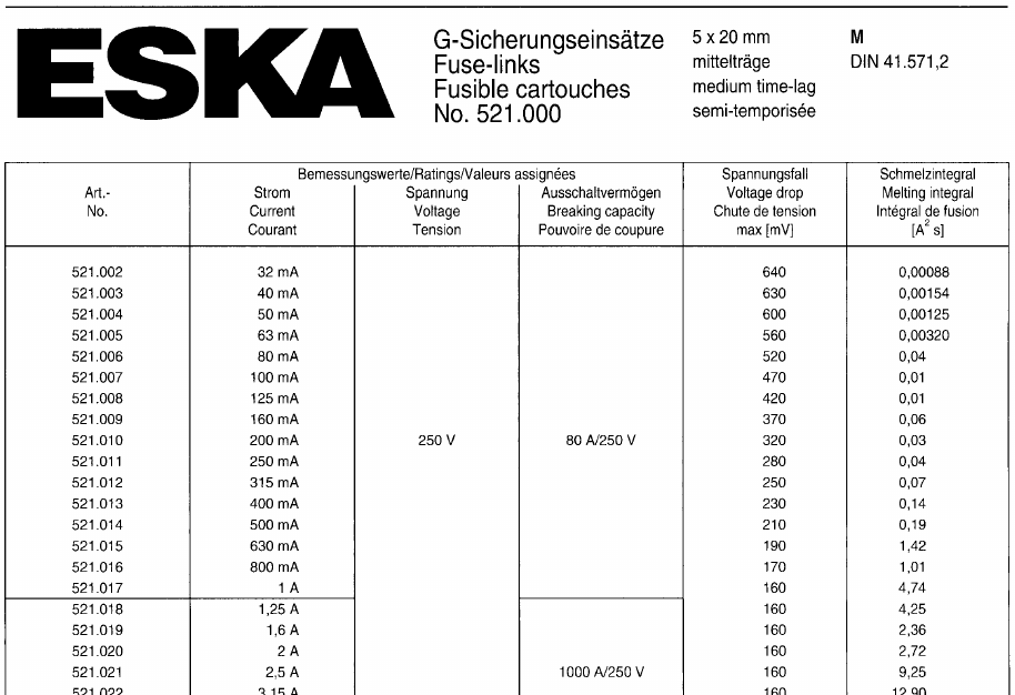
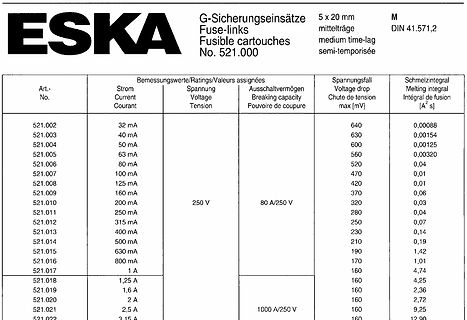
Datenblatt Tabelle ESKA Fuse-links
Ausschaltvermögen Breaking capacity Pouvoir de coupure Spannungsabfall Voltage drop Chute de tension max [mV] Schmelzintegral Melting integral ∫ fusion [A²s] 521.002 32 mA 640 0,00088 521.003 40 mA 630 0,00154 521.004 50 mA 600 0,00125 521.005 63 mA 560 0,00320 521.006 80 mA 520 0,04 521.007 100 mA 470
in „TVS Diode wir bei Überspannung zerstört“ · Analoge Elektronik und Schaltungstechnik · · Screenshots
-
 Bild
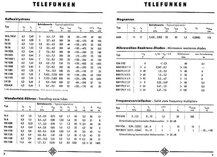
Tabellen mit technischen Daten von Reflexklystronen und Magnetron
Typical operation Typ Uf If f Ures Ires Urfl Δf/f NHF TK6 TK61 6,3 0,40 3 GHz 6,5...7 300 28 -50...-190 49 TK8 6,3 0,38 3 GHz 3,7...4 300 28 -60...-170 58 TK75 6,5 1,55 2,3 GHz 3,5...4 300 52 -450...-470 33 YK1020 6,3 0,44 2 GHz 7,6...8 300 -280...-260 25 YK1021 6,3 0,44 2 GHz 6,5...7 300 -75...-225 100
in „Hilfe bei Bauteilidentifizierung“ · HF, Funk und Felder · · Screenshots
-
PDF
LT1734.pdf
TYPICAL PERFOR A CE CHARACTERISTICS IBAT2 vs Temperature and Supply Voltage IBAT1 vs V BAT IBAT2 vs VBAT 190 52 190 RPROG = 2.1k VCC = 5V VCC = 5V PNP = FCX589 T = 25°C T = 25°C RA = 7.5k RA = 2.1k PROG PROG PNP = FCX589 PNP = FCX589 ) ) A A A BAT PIN MUST BE DISCONNECTED ( ( ( AND GROUNDED TO FORCE T180 V
in „akku mit solar aufladen, kommt das IC: LT1734L dafür in Frage?“ · Analoge Elektronik und Schaltungstechnik ·
-
PDF
MCP73831.pdf
VIEW TOP VIEW EXPOSED A1 A TIE BAR A3 (NOTE 3) Units INCHES MILLIMETERS * Dimension Limits MIN NOM MAX MIN NOM MAX Number of Pins n 8 8 Pitch e .020 BSC 0.50 BSC Overall Height A .031 .035 .039 0.80 0.90 1.00 Standoff A1 .000 .001 .002 0.00 0.02 0.05 Contact Thickness A3 .008 REF. 0.20 REF. Overall Length
in „Akku Ladetechnik“ · Mikrocontroller und Digitale Elektronik ·
-
PDF
SSD1303.pdf
.................................... 3. Revise Max t , t RromF15ns to 40ns in Table 11 - 8080-Series MPU Parallel Interface Timing Characteristics .......................................................................................................................................... 4. Revise Max t , t RromF15ns to 40ns in Table 12 – Serial Interface Timing Characteristics.....................d Table 1 - Ordering Information....................................................................
-
PDF
verfahren_zur_darstellung_von_segelflugpolaren.pdf
0,0425 ( 4,8 % ) 140 1,2400 0,0000 ( 0,0 % ) 160 1,8475 -0,0975 ( -5,6 % ) 180 2,6700 0,0000 ( 0,0 % ) 190 3,1619 0,0281 ( 1,0 % ) 5 0 -5 av²+bv+c -10 -15 70 80 100 120 140 160 180 km/h Abbildung 3 Die Fehlerverteilung der Quadratfunktion Von den Geschwindigkeitswerten zwischen 70 und 90 km/h einmal abgesehen
in „AVR: Interpolation? Splines?“ · Mikrocontroller und Digitale Elektronik ·
-
PDF
aqh3213.pdf
Through hole terminal type Surface-mount terminal type External dimensions External dimensions CAD CAD MAX.10° MAX.10° 2 . . 6 7 MAX.10° . 6 Recommended mounting pad 6 7 9.78 3.4 PC board pattern . (TOP VIEW) ± 1 (BOTTOM VIEW) . 9.78 3.4 3 7-0.8 dia. hole 4 7.62 0 3 2.54 3 . 8 . 0.5 0.5 0.5 0.5 + − 2 0.5
in „230V LED-Lampe (kleiner Strom) schalten (SSR, Optotriac,.)?“ · Mikrocontroller und Digitale Elektronik ·
-
PDF
P4SMA_LIF.PDF
FBEoGSFF▯BTTFNCMZ t TP p -Temperature Min (T ) 150°C s(min) Ramp-up CTito Tl Zone Pre Heat -Temperature Max (T ) 200°C TL L P s(max) ) tL -Time (min to max) (t ) ▯▯▯o▯▯▯▯▯TFDT (Ts(max) s u Average ramp up rate (LiquidusTemp r Ramp-down 3°C/second max pTs(min) (TL) to peak m s T Preheat TS(max)oTL- Ramp-up Rate 3°C/second max -Temperature (T L (Liquidus) 217°C 25˚C t 25˚C to Peak Reflow -Time (min to max) (ts) ▯▯▯o▯▯▯▯▯TFDPOET Time (t) +0/-5 PeakTemperature (T )P 260 °C Time within 5°C of actual peak ▯▯▯o▯▯▯▯TFDPOET Temperature
in „Warum noch KFZ-Relais?“ · Analoge Elektronik und Schaltungstechnik ·
-
PDF
Feinsicherung-520.600-AC-5-x-20-mm-flink-ESKA.pdf
Bemessungswerte / Ratings: I - t Verhalten / I - t characteristics: N N BC_AC / 2 Art. No. I U N_AC / DC U d_max P d_max I t Bemessungs- Schmelzzeit N [V] [mV] [W] DC [A s] [A] strom-Faktor / 520.602 2) 32 mA 250 / 60 10.000 1,6 35 / 0,32 0,00008 / Melting time: 2) Rated current 520.603 40 mA 250 / 60 8.000 1,6
in „TVS Diode wir bei Überspannung zerstört“ · Analoge Elektronik und Schaltungstechnik ·
-
Datei
hope.c
Bestimmung des Messkanls /-----------------------------------------------*/ unsigned int adc_voltage_max_value(unsigned char channel2) { unsigned int i, result; unsigned int max=0; uint32_t voltagemax = 0; ADMUX = (ADMUX & ~(0x1F)) | (channel2 & 0x1F);// Kanal waehlen ADCSRA |= (1<<ADSC); while ( ADCSRA
in „Atmega88 region text overflowed by 156 bytes“ · Mikrocontroller und Digitale Elektronik ·
-
PDF
E-Cap_Miniature_SC_2011.pdf
0.6 . . 10.0 5.0 5 5 12.0 L 15Min. 5Min. D±0.5 L 15Min.5Min. D±0.5 13.0 16.0 7.5 0.8 L≤ 16 L + 1.5Max. Dø < 20 Dø + 0.5 L> 16 L + 2Max. Dø ≥ 20 Dø + 1 18.0 Dø = 8 & 10 L + 2.5Max. 22.0 10.0 0.8 (1.0) 61 CASE SIZE & PERMISSIBLE RIPPLE CURRENT OF STANDARD PRODUCTS D x L:mm CAP.(µF) RATEDVOLTAGEWV (SURGEVOLTAGEWV
in „TFT Monitor Elkos“ · Analoge Elektronik und Schaltungstechnik ·
-
PDF
IXTA-TP3N50D2_.pdf
42 ns Side f Q g(on) 40 nC Dim. Millimeter Inches Q gs V GS = 5V, V DS = 250V, I = D.5A 5 nC Min. Max. Min. Max. Q 20 nC A 4.06 4.83 .160 .190 gd b 0.51 0.99 .020 .039 b2 1.14 1.40 .045 .055 R thJC 1.00 °C/W c 0.40 0.74 .016 .029 c2 1.14 1.40 .045 .055 R thCS TO-220 0.50 °C/W D 8.64 9.65 .340 .380 D1
in „J-FET N-Channel mit gößer 70V Drain / Source Spannung für Konstantstromsenke“ · Analoge Elektronik und Schaltungstechnik ·
-
PDF
1.5KE6V8A.PDF
and 7. DS21503 Rev. 10 - 2 1 of 4 1.5KE6V8(C)A - 1.5KE400(C)A www.diodes.com ã Diodes Incorporated Max. Max. Max. Type Type Reverse Breakdown Voltage Reverse Clamping Max. Voltage Number Number Standoff V @ I Current Leakage Voltage Pulse Temp. (Note 1) (Note 1) Voltage BR T (Note 2) @ I Current Variation @ V R pp of VBR (UNI) (BI) VRWM (V) Min (V) Max (V) It(mA) R (mA) V CV) PP (A) %/°C 1.5KE6V8A 1.5KE6V8CA 5.80 6.45 7.14 10 1000 10.5 143.0 0.057 1.5KE7V5A 1.5KE7V5CA 6.40 7.13 7.88 10 500 11.3 132.0 0.061 1.5KE8V2A 1.5KE8V2CA 7.02 7.79 8.61 10 200
in „Welches Bauteil (Diode?) ist das?“ · Analoge Elektronik und Schaltungstechnik ·
-
Datei
Configuration_adv.h
its usage. */ //#define MAX7219_DEBUG #if ENABLED(MAX7219_DEBUG) #define MAX7219_CLK_PIN 64 #define MAX7219_DIN_PIN 57 #define MAX7219_LOAD_PIN 44 //#define MAX7219_GCODE // Add the M7219 G-code to control the LED matrix #define MAX7219_INIT_TEST 2 // Test pattern at startup: 0=none, 1=sweep, 2=spiral #define MAX7219_NUMBER_UNITS 1 // Number of Max7219 units in chain. #define MAX7219_ROTATE 0 // Rotate the display clockwise (in
in „Ender3 Z-Achse fährt mit Marlin nur nach oben“ · Mechanik, Gehäuse, Werkzeug ·
-
PDF
Relais-Carlo-Gavazzi-MZP-R2.pdf
Max. switching voltage (VDE 0435) 380 VAC 380 VAC 380 VAC Max. switching powe3)with resistive load in AC 1250 VA 2500 VA 4000 VA Max. switching power in DC see diagram 3 see diagram 3 see diagram 3 Life ( see diagram 1) Expected life at max. resistive load and repetition at: 1000 cycles /h 3 x 10 5 2 x 10 5 3 x 10⁵ 7.5 x 10⁴ 10 cycles 500 cycles/h 3.5 x 10⁵ 2.5 x 10⁵ 3.5 x 10⁵ 8 x 10⁴ 1.5 x 10⁵ Max. electrical repetition rate 3600 cycles
in „24V Relais ansteuern“ · Analoge Elektronik und Schaltungstechnik ·
-
PDF
3260__1_.pdf
0,159 4,04 0,062 45° 1,57 0,058 45° 1,47 0,122 3,10 0,117 2,97 45° 45° 0,031 0,79 0,085 123 2.16 123 MAX MAX 0,640 0,0173 16,26 0,44 0,600 0,0138 15,24 0,35 0,0189 0,48 SIEHE HINWEIS SIEHE HINWEIS 0,0142 0,36 0,050 1.27 BSC Zeichnung MH-014E in BSC Zeichnung MH-014E mm Oberflächenmontierte Anschlussform (Suffix „-TL“) 0,095 2,41 ±0,005 ±0,13 0,002 0,051 MAX MAX 0,004 0°–8° 0,10 0°–8° MAX 0,020 MAX 0,51 MIN MIN WOHNUNG Zeichnung MH-015 in FLACH Zeichnung MH-015 mm HINWEISE: 1. Toleranzen bei Pakethöhe und -breite stellen zulässige Formversätze dar. Die
in „Schaltnetzteil TNY Ersatztyp Kompatibel ?“ · Analoge Elektronik und Schaltungstechnik ·
-
PDF
emmc.pdf
62] FFFh Maximum read current at VDD,min VDD_R_CURR_MIN 3 R [61:59] 7h Maximum read current at VDD,max VDD_R_CURR_MAX 3 R [58:56] 7h Maximum write current at V VDD_W_CURR_MIN 3 R [55:53] 7h DD,min Maximum write current at DD,max VDD_W_CURR_MAX 3 R [52:50] 7h Device size multiplier C_SIZE_MULT 3 R [49
in „Pin-Swap/Cross IC?“ · Mikrocontroller und Digitale Elektronik ·
-
Datei
tonleiter.asm
Übergabewert temp1 ist 127 entspricht 1 Oktave ;; Minimale Frequenz 440Hz @4MHz => temp2 = 4MHz/2/440/temp1_max/3-1= 5 WAIT: _WAIT1: ldi temp2, $05 ;(1)*temp1 _WAIT2: dec temp2 ;(1)*temp2*temp1 brne _WAIT2 ;((2)*temp2-(1)) * temp1 dec temp1 ;(1)*temp1 brne _WAIT1 ;(2)*temp1-(1) ret tonleiter: ;; c d e f g a h c Terminierung .db 254, 226, 202, 190, 170, 151, 135, 127, 0
in „Tonleiter erzeugen“ · Mikrocontroller und Digitale Elektronik ·
-
Datei
tonleiter.asm
Übergabewert temp1 ist 127 entspricht 1 Oktave ;; Minimale Frequenz 440Hz @4MHz => temp2 = 4MHz/2/440/temp1_max/3-1= 5 WAIT: _WAIT1: ldi temp2, $05 ;(1)*temp1 _WAIT2: dec temp2 ;(1)*temp2*temp1 brne _WAIT2 ;((2)*temp2-(1)) * temp1 dec temp1 ;(1)*temp1 brne _WAIT1 ;(2)*temp1-(1) ret tonleiter: ;; c d e f g a h c Terminierung .db 254, 226, 202, 190, 170, 151, 135, 127, 0
in „Tonleiter erzeugen“ · Mikrocontroller und Digitale Elektronik ·
-
Datei
SensorMeasurements.m
60cm distance, maximum at circa 40.4kHz'); angle = -90:5:90; ampl = [570 560 540 500 430 390 320 265 190 145 100 73 55 49 45 47 47 42 43]*0.001; ampl = [fliplr(ampl(2:length(ampl))) ampl]; ampl = 20*log(ampl/max(ampl)); figure(2); plot(angle, ampl); grid on; xlabel('Angle / \circ'); ylabel('Attenuation
in „Ultraschallsensoren des HC-SR04 Moduls“ · Projekte & Code ·
-
Datei
SensorMeasurements.m
60cm distance, maximum at circa 40.4kHz'); angle = -90:5:90; ampl = [570 560 540 500 430 390 320 265 190 145 100 73 55 49 45 47 47 42 43]*0.001; ampl = [fliplr(ampl(2:length(ampl))) ampl]; ampl = 20*log10(ampl/max(ampl)); figure(2); plot(angle, ampl); grid on; xlabel('Angle / \circ'); ylabel('Attenuation
in „Ultraschallsensoren des HC-SR04 Moduls“ · Projekte & Code ·
-
PDF
085cs.pdf
electrolytic capacitors 085 CS SMD (Chip) Standard MECHANICAL DATA handbook, halfpage handbook, halfpage 2 max 2 max max9 2 max 2 max max9 2.7 2.7 2.7 2.7 max max max max 4.1 3.9 4.1 3.9 max max max max 7.5 10.8 9 max MGB099 - 1 12.2 max MGB100 - 1 a. b. Dimensions in mm. a. Case size 8.8 × 3.7 × 3.9 mm. b.
in „Tantal vs Kerko“ · Analoge Elektronik und Schaltungstechnik ·
-
PDF
BMA020_DataSheet_1.1_080114.pdf
sheet BMA020 Bosch Sensortec Digital, triaxial acceleration sensor Parameter Symbol Condition Min Typ. Max Units Bandwidth bw 2 order analog 1500 Hz filter Digital filter 25, 50, 100, Hz 190, 375, 750 Acceleration data f_rate 2700 3000 3300 Hz refresh rate (all axes) Nonlinearity NL Best fit straight lin
in „Über Mikrocontroller Beschleunigungssensor auslesen“ · Mikrocontroller und Digitale Elektronik ·
-
PDF
BMA020_DataSheet_1.1_080114.pdf
sheet BMA020 Bosch Sensortec Digital, triaxial acceleration sensor Parameter Symbol Condition Min Typ. Max Units Bandwidth bw 2 order analog 1500 Hz filter Digital filter 25, 50, 100, Hz 190, 375, 750 Acceleration data f_rate 2700 3000 3300 Hz refresh rate (all axes) Nonlinearity NL Best fit straight lin
in „Bosch BMA020 Zweierkomplement“ · Mikrocontroller und Digitale Elektronik ·
-
PDF
ONS21800604.pdf
Lead* 500 Units/Box (Lead Length w 1/16″ from Case, 10 s Max) Stresses exceeding Maximum Ratings may damage the device. Maximum MKP3V240G Axial Lead* 500 Units/Box Ratings are stress ratings only. Functional operation above the Recommended Operating Conditions
in „Innenleben von HQI Zündgeräten??“ · Analoge Elektronik und Schaltungstechnik ·
-
PDF
IPB180P04P4.pdf
Data Sheet IPB180P04P4L-02 ® OptiMOS -P2 Power-Transistor Product Summary V DS -40 V R 2.4 DS(on),max mW ID -180 A Features PG-TO263-7-3 • P-channel - Logic Level - Enhancement mode • AEC qualified • MSL1 up to 260°C peak reflow • 175°C operating temperature • Green Product (RoHS compliant) • 100% Avalanche
in „wie pMOSFET für Strombegrenzung kühlen“ · Analoge Elektronik und Schaltungstechnik ·
-
PDF
FS277-FeelingTechnology.pdf
) P3/FS277 o DC Electrical Characteristics (at Ta = 25 C) PARAMETER SYMBOL TEST CONDITIONS MIN TYP MAX UNIT Operating Voltage V No use pin is open (Fig1) 3 - 20 V CC No use pin is open V : 3V Quiescent Supply current ICC cc - 18 20 mA to 20V (Fig1) Output Leakage current Ileak Vcc=12V, Vce=20V - <0.1
in „Bauteil Identifikation“ · Mikrocontroller und Digitale Elektronik ·
-
PDF
S-350-27_datasheet.pdf
0 ~ 9.7A 0 ~ 7.3A RATED POWER 250W 300W 348W 348.3W 348W 350.4W 351W 349.2W 350.4W RIPPLE & NOISE (max.)Note.2150mVp-p 150mVp-p 150mVp-p 150mVp-p 150mVp-p 150mVp-p 200mVp-p 240mVp-p 240mVp-p OUTPUT VOLTAGEADJ. RANGE 4.5 ~ 5.6V 6 ~ 9V 10 ~ 13.2V 12 ~ 15V 13.5 ~ 18V 20 ~ 26.4V 26 ~ 32V 32~40V 41 ~ 56V
in „[V] 14 Netzteile 27V 13A“ · Markt ·
-
PDF
recommended.pdf
maintain regulation depends on the load current and output voltage, and is calculated as: V Iin = V O max + I O max× r( DS(on) max + R (L) ) (2) with: IOmax = maximum output current plus inductor ripple current r max = maximum P-channel switch r DS(on) DS(on) R (L) dc resistance of the inductor V Oax =
in „Kurz vorm Verzweifeln“ · Analoge Elektronik und Schaltungstechnik ·
-
PDF
TPS6211.pdf
maintain regulation depends on the load current and output voltage, and is calculated as: V Iin = V O max + I O max× r( DS(on) max + R (L) ) (2) with: IOmax = maximum output current plus inductor ripple current r max = maximum P-channel switch r DS(on) DS(on) R (L) dc resistance of the inductor V Oax =
in „DC DC Wandler Pins“ · Analoge Elektronik und Schaltungstechnik ·
-
PDF
TPS6211.pdf
maintain regulation depends on the load current and output voltage, and is calculated as: V Iin = V O max + I O max× r( DS(on) max + R (L) ) (2) with: IOmax = maximum output current plus inductor ripple current r max = maximum P-channel switch r DS(on) DS(on) R (L) dc resistance of the inductor V Oax =
-
PDF
TPS6211.pdf
maintain regulation depends on the load current and output voltage, and is calculated as: V Iin = V O max + I O max× r( DS(on) max + R (L) ) (2) with: IOmax = maximum output current plus inductor ripple current r max = maximum P-channel switch r DS(on) DS(on) R (L) dc resistance of the inductor V Oax =
in „QFN Gehäuse.“ · Analoge Elektronik und Schaltungstechnik ·
-
PDF
TPS6211.pdf
maintain regulation depends on the load current and output voltage, and is calculated as: V Iin = V O max + I O max× r( DS(on) max + R (L) ) (2) with: IOmax = maximum output current plus inductor ripple current r max = maximum P-channel switch r DS(on) DS(on) R (L) dc resistance of the inductor V Oax =
in „Trennung von analoger und digitaler Spannung“ · Analoge Elektronik und Schaltungstechnik ·
-
Datei
FastSoftPWM.asm
process_ltbl1 ;continue with processing if length indicator >0 ret process_ltbl1: mov r16,r25 andi r25,15 ;max. length needed for 256 LEDs is 2048 bytes andi r16,$f0 sts (probability),r16 ;upper 4 bits for definition of probability in random mode elpm r16,Z+ ;read duration low byte st Y+,r16 elpm r16,Z+ ;read