Anlage automatisch in den Sleep-Modus Was bereits funktioniert: - Wemos D1 Mini (ESP8266) - PN532 über I²C - NFC-Tags werden zuverlässig gelesen - DFPlayer Mini + microSD - MP3-Wiedergabe funktioniert - Die Software-Logik (NFC → bestimmter Track → Wiederholungen → Sleep) ist praktisch fertig
so nah wie möglich bei null liegen" soll, kannst du überlegen ob der "Hard Power Down"-Modus vom PN532 noch akzeptabel ist, oder ob du lieber den Strom ganz abdrehst. Auch den Querstrom von mglw. auf den China-Breakout-Boards verbauten LDO berücksichtigen.
i R t S i a e l . B z K W m l a o p n u 8 q n e I l m . f a p 4 e i E e i d e M g u t e E i l . e ad u z i n . r - T e l H b ä o z : A u / o w d e h u i d Q n s t / d N i w z C W ü TmAS5/5T e M te i L a B i i a e e n S t d c e t B i D c g e T Z b D3 G A m e s r 2 V w n b b b n S g i a 2 W e r g i U
Sound of an inrush current into a 40MVA Power Transformer. #electricity #transformers #energy 209.532 Aufrufe https://www.youtube.com/shorts/SY5ai6YkCbY Der Vorteil aller Schaltungen ist, dass der Trafo dann richtig steif ausgelegt werden kann, wodurch man einen hohen Wirkungsgrad erzielt. Denn
den G* > bei jeder Suchanfrage vorneweg präsentiert. Seit letzter Zeit scheint der @P auf das "ad hominem" eingeschossen zu sein. R. L. schrieb im Beitrag #8054205: > fachliche Kompetenz kann man verbessern, bei sozialer Kompetenz ist das > anscheinend nicht möglich. Ich würde das nicht so
VCC ) voltage is then adjusted to provide a code change from FE HEX to FFHEX . This completes the ad- for VREF /2 2.500 V DC). justment procedure. 2.5.2 Full-Scale 2.6 Clocking Option The full-scale adjustment can be made by applying a differ- The clock for the A/D can be derived from the CPU clock
. . . e e e e e e es OD bon 1.4.3.2. Time measurements 2... 0... 0. e c e e e e ee eee eee eee ee AD 1.4.3.3. Trigger measurements .. 0.0.00... c c c e e ee ee eee ee eee eee 40 : 1.4.4. Analog section (multifunction measurements) . . . . .00.600.0 e.ee0ee. ac.es Af : 1.4.4.1, R M S . convertor 2 .
ee ec eet et eee e e e n s 42 4 2 4 , Initial test e e e e e e e e e c e c e oe e e e e e c t e e e AD 4 2 2 . Function pert t e s t . . . oe oe ee ee cence cece e eens eee te rene eee t e n e s 4B 423, V em V an,d 1 > preset test... 0... e e e e cece e e e e e e e e e Ao 424. Vac part test ooo. ee c
SUPPLY VOLTAGE: -8 kV I T 0 200 250 300 350 400 450 AD REVERSE BIAS VOLTAGE (V) THBV4_1208EA Figure 12-8:Time response characteristics vs. AD reverse bias voltage On the other hand, when the photocathode supply voltage is changed while the AD reverse bias
0xA8 Register_A9 data 0xA9 Register_AA data 0xAA Register_AB data 0xAB Register_AC data 0xAC Register_AD data 0xAD Register_AE data 0xAE Register_AF data 0xAF P3 data 0xB0 Register_B1 data 0xB1 Register_B2 data 0xB2 Register_B3 data 0xB3 Register_B4 data 0xB4 Register_B5 data 0xB5 Register_B6 data 0xB6
in Quarantäne, gerade das von dir genannte HyperCam ist ja mittlerweile die reinste BloatWare und AdWare Schleuder. Das möchte man tatsächlich nicht auf seinem Rechner haben. Aber klar - wenn du unbedingt magst: hebe die Quarantäne auf! Ich freue mich dann schon auf deinen nächsten Flamethread: "
STOP bit AD AD AD AD 0 0 x D8 A D7 D6 D5 D4 D3 D2 D1 D0 A P 3 2 1 0 WRITE Command Write Data bits Note: Only functions when writing the volatile wiper registers (AD3:AD0 = 00h, 01h, and 04h) or the TCON register
the four terms u , I , u C2 A C3 and I B While u C2 and u C3 are already known, two formulas for I aAd I areBnecessary. These formulas can be easily determined from Figure 33 and Figure 34 and are IA= i L4 , IB= i L3· α. (42) The equations for the output vector y(t) must also be de▯ned and depend on which
P P 0 1 0 1 1 0 10 10 1 0 P P P P 1 0 1 0 1 0 1 0 P P P P P P P0C12801P0C12802 P0VR10101 0 P0D1050AD105P0D1060A0D106P0D1070A0D107P0D1080AD1080P0D1090AD109P0D1100A0D110P0D1110AD1110K 2 2 3 3 4 4 P0D115P00AD1150PK0D1160PA0D1160PK0D1170PA0D1170PK0D1180PA0D1180K 9 9 0 0 P0D1210PA0D1210PK0D1220PA0D1220PK0D1230PA0D1230PK0D124P00AD1240PK0D1250PA0D1250PK0D1260PA0D1260K
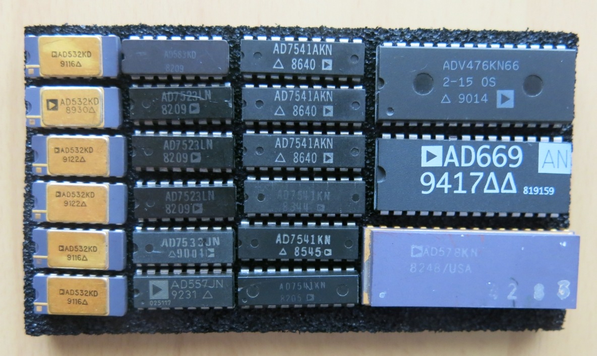
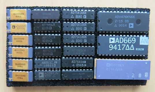
Hallo zusammen, ich möchte noch ein Konvolut alter ICs von Analog Devices anbieten: 6 x AD532, analog Multiplier 1 x AD583, Sample-and-Hold amplifier 4 x AD7523, 8-bit multiplying DAC 1 x AD557, 8-bit DACPORT 6 x AD7541, 12-bit multiplying DAC 1 x ADV476, Video RAM-DAC 1 x AD578, 12-
hättest du klar kommunizieren können, a la "Kann es sein, dass du den Thread verwechselt hast, den AD-Krams hatte ich bestellt". Das wäre dann aber nicht so schön dispektierlich. Alternativ wäre noch so etwas wie "Ey du Vollhorst, ICH habe die AD-Sachen bestellt, schreib in deinen Thread" denkbar
fulDDVON-OFF-ON cycle. e • Under 16-bit bus mode and CD=0, D[15:8] is ignored and only D[7:0] is used. Ad a result, the bus cycles for commands under 16-bit bus and 8-bit bus are the same, and double-byte commands stillineed two bus cycles under 16-bit bus mode. Example: f 8-bit bus mode: n Set PL[1:0] =
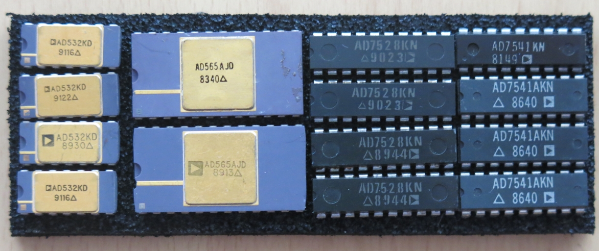
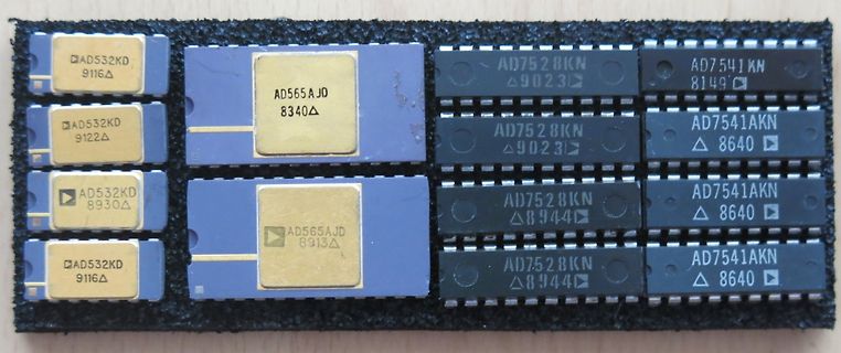
Hallo zusammen, ich möchte ein Paar alten ICs von Analog Devices anbieten: 4 x AD532, analog Multiplier 2 x AD565, 12-bit DAC 4 x AD7528, dual 8-bit multiplying DAC 4 x AD7541, 12-bit multiplying DAC Zustand: entsockelt vor ca. 20-25 Jahren, ESD-konform aufbewahrt Preis
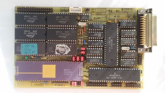
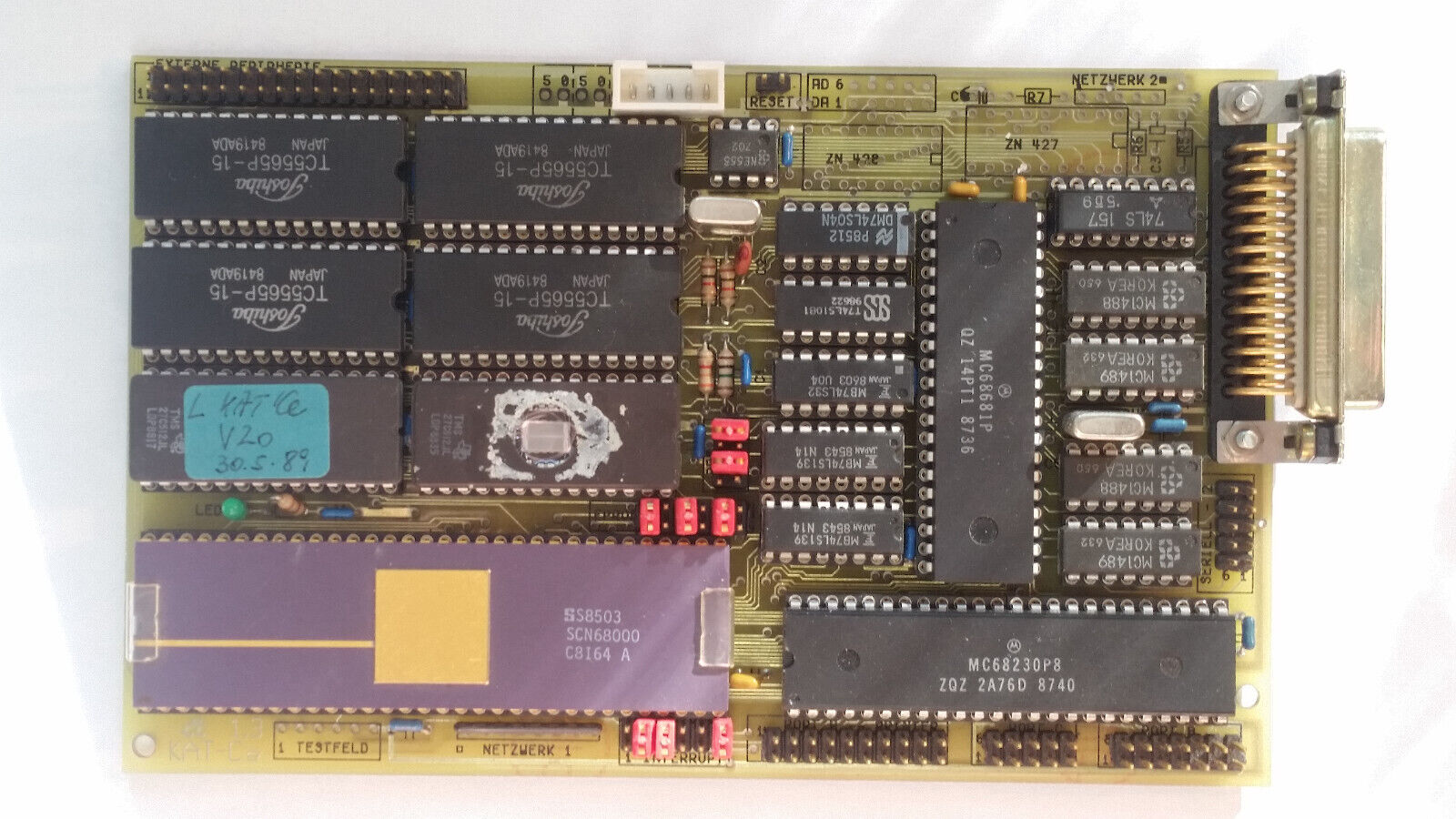
TC5655P-15 JAPAN 841A DA, Toshiba TC5655P-15 JAPAN 841A DA, Toshiba TC5655P-15 JAPAN 841A DA, RESET, AD 6, NETZWERK 2, ZN 427, 74LS 157, MC1489 KOREA 650, MC1489 KOREA 652, MC1489 KOREA 659, MC1489 KOREA 652, MC68117 8736, MC68230P8 ZQ2 2A76D 8740, 8874L532, 8874L539, 8874L539, 8874L539,
C/W TO-243AA (SOT-89) 133 C/W Electrical Characteristics (Test conditions unless otherwise specifiAd: -40°C < T < 85°C.) Sym Parameter Min Typ Max Units Conditions V - V Input to output voltage difference 12 - 450 V --- IN OUT 13.2V < V < 400V, 1.14 1.20 1.26 V IN VOUT Overall output voltage regulation
See replacement. Consult Marketing. 74LVC10D 74LVC10D LVC 935205880118 T M 2 31-12-00 30-6-01 74LVC10AD Name change only. See replacement. Consult Marketing. 74LVC10D 74LVC10D LVC 935205880112 T M 2 31-12-00 30-6-01 74LVC10AD Name change only. See replacement. Consult Marketing. 74LVC10DB 74LVC10DB LVC
AB : B772 IN R23,TCNT0 ; capture timer0 low byte 351/ AC : 1581 CP R24,R1 ; check for overflow 352/ AD : F7E1 BRNE DO_PW2 ; if yes, then capture again 353/ AE : 9990 SBIC MOTPRT,MOTPWM ; test motor control bit 354/ AF : C004 RJMP PWM_OF ; if set, then goto motor off 355/ B0 : 9A90 PWM_ON: SBI MOTPRT,MOTPWM
P353 M532 Querregeltransformatoren (PST) Abzweig Waldeck2 (ehemals Twistetal) (Ad-hoc-Maßnahme) P359 M571 Stendal/West – Wolmirstedt P360 Anlagen zur Bereitstellung von Blindleistung und Momentanreserve in der
> Unter anderem einen ICL8038 Den gibt es aber nur noch im Museum. In Produktion ist z.B. der AD9837.
immer riesige Programme schreiben. Erst wenn dann noch weitere große Libs dazukommen (z.B. für die AD-Converter), dann erst könnte es knapp werden. VG Andreas PS: warum willst Du nicht auf den Arduino Mega 2560 wechseln? Formfaktor zu groß?
Semiconductor National Semiconductor Corporation Europe Hong Kong Ltd. Japan Ltd. Arlington, TX 76017ad Email: cnjwge@tevm2.nsc.com Ocean Centre, 5 Canton Rd., Fax: 81-043-299-2408 Tel: 1(800) 272-9959 Deutsch Tel: (+49) 0-180-530 85 85 Tsimshatsui, Kowloon Fax: 1(800) 737-7018 EnglishTel: (+49) 0-180-532 78 32 Hong Kong ItalianTel: (+49) 0-180-534 16 8058 Fax: (852) 2736-9960 www.national.com National does not assume any responsibility for use of any circuitry described, no circuit patent licenses are
LM361N CAEN fire part.. CAEN Fire part. No possibility of further Philips manufacture due to 150 NE532D NE532 D LINEAR INDUSTRIA L 933656080602 T M 1 20-feb-04 20-feb-04 ON Semi: LM358D CAEN fire. No possibility of further Philips manufacture due to 151 NE532D NE532 D LINEAR INDUSTRIA L 933656080623
OR INT E R NAT IONAL PAR T NU MB E R R E CT IF IE R F 530S L OGO DAT E CODE P = DE S IGNAT E S L E AD-F R E E L OT CODE L Y PR ODU CT (OP T IONAL ) YE AR 0 = 2000 WE E K 02 A = AS S E MB L Y S IT E CODE 8 www.irf.com IRF3708/S/LPbF TO-262 Package Outline IGBT 1- GATE 2- COLLECTOR 3- EMITTER TO-262 Part
T a b le 6 -3 . T ab le 6 -3 S ettin g o f A D D R E S S S w itch GPIB B it GPIB B it GPIB B it 1 ad d ress 5 4 3 2 1 ad d ress 5 4 3 2 1 ad d ress 5 4 3 2 0 0 0 0 0 0 0 0 0 0 1 11 0 1 0 1 1 21 1 0 1 0 . 2 0 0 0 1 0 12 0 1 1 0 0 22 1 0 1 1 0 3 0 0 0 1 1 13 0 1 1 0 1 23 1 0 1 1 1 4 0 0 1 0 0 14 0 1 1

 Bild
Bild
 Bild
Bild
 Bild
Bild