1 r t r) rrieb ligrkorew (lo f 3 i g le ta ,liftinr,tran letae mre In )gn (lokc r,tran letaem re :inaC D NG 6 2 l 0 W i x -x11363 00 42P 3 X d i NI 2 a L b r) rrieb ligkfoepp (u )gn (lo kc r,tran leae m re :ineaC n g le ta ,liftin r,tran letaem re In D NG 6 1 i u I x -x11363 00 42P 3 X r t T NI 2 v
Zeit/Datum bekommt man auch über die Funkrundsteuerung (drei Sender im Bereich 129,1 kHz bis 139 kHz). Die Dekodierung ist problemlos, die Zeit wird normalerweise alle 10 Sekunden übertragen. https://de.wikipedia.org/wiki/Funkrundsteuertechnik Für eine hochgenaue Referenz nicht
Beitrag #8051837: > Zeit/Datum bekommt man auch über die Funkrundsteuerung (drei Sender im > Bereich 129,1 kHz bis 139 kHz) Christoph M. schrieb im Beitrag #8051842: > 2009 habe ich mir eine DCF-Uhr mit einem Atmega8 mit eigenem Code, der > auch wichtige Geburtstage fest drinn hat Sehr schön, jetzt
T32A05INB1/T32A05INC0/T32A05INA0/ 143 USB_VBUS_PRT +3.3S_PON I I USB Power Feedback AINA10/PP2 144 T32A05INA1/T32A05INC1/T32A05INB0/ TEST1 +3.3S_PON I I AINA11/PP3 145 T32A06INB1/T32A06INC0/T32A06INA0/ MODE +3.3S_PON I I AINA12/PP4 T32A06INA1/T32A06INC1/T32A06INB0/ 146 AINA13/PP5 TEST2 +3.3S_PON I I T32A07INB1/T32A07INC0/T32A07INA0/ 147 STBY_LED AC O O Standby LED control INT10b/AINA14/PP6 148 T32A07INA1/T32A07INC1/T32A07INB0/ DSP2_NIC
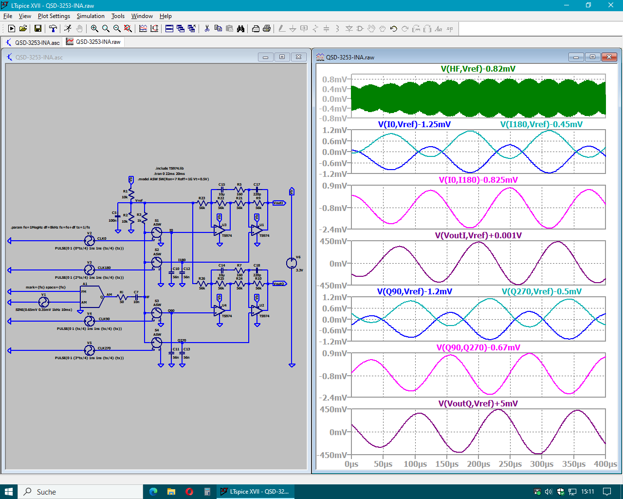
erreicht werden. Der größere Unterschied kann ja kaum vom in der Praxis besseren INA als der idealisierten Simulation des INA stammen.
Werte erreicht werden. Der > größere Unterschied kann ja kaum vom in der Praxis besseren INA als der > idealisierten Simulation des INA stammen. Was ist mit diesen Worten gemeint?
ISOW7843, ISOW7844 www.ti.com SLLSEY2G – MARCH 2017 – REVISED AUGUST 2021 VCC 1 16 V ISO GND1 2 15GND2 INA 3 14 OUTA N I INB 4 T 13 OUTB L INC 5 O 12 I OUTC OUTD 6 11 IND NC 7 10 SEL GND1 8 9 GND2 Figure 6-2. ISOW7841 DWE Package 16-Pin SOIC-WB Top View VCC 1 16 V ISO GND1 2 15GND2 INA 3 14 OUTA N I INB
input current goes up by a factor of 2.3 every 10 °C, as shown in Figure 1.2 [38]. 23 _· ~ _~~~~~~~~~ InA ItA __ _ _____ - IooA -5s -25 5 is O M 1~23 TEPtIATUR- 'C Figure 1.2: Leakage current versus temperature for AD549 op-amp [38] 1.2.2 VOLTAGE OFFSET The voltage offset of an op-amp is made up of two
iwas.. was ich halt via UART oder I2C auslesen > kann. ??? UART wirst du wohl kaum finden. INA129 mit I2C/SMBUS? Bei deiner Spannung kann der allerdings wohl den Strom nicht High-Side messen. Oder wie ernst ist deine Angabe "24V" zu nehmen?
Hammer einschlagen. Aber es gibt für Dein Problem eben auch geeignetere Werkzeuge. Beispielsweise INA238 (16 Bit Auflösung) https://www.ti.com/lit/ds/symlink/ina238.pdf oder INA228 (20 Bit Auflösung). https://www.ti.com/lit/ds/symlink/ina228.pdf Die messen direkt Spannung und Strom und errechnen
possibleinclination. • The heated air mustdissipate unhindered (fig. d,page 7). • Wheninstallingthe coolingunit ina closed room suchas a wardrobe, pantry or aftcompartment,openingsmusthavea crosssectionof at least 200 cm² (25cm x 8cm) for cooling and exhaust air. • Makesurethattheairflowonthecondenser(fig.d C,page
Periodic Rectangular Pulse T = P ×Z = 100×0.04 = 4°C j −mb thj −mb Whenconsidering thejunctiontemperature ina device,the The value for Z th j-mb taken from the δ=0 curve shown in following formula is used: Fig. 12.Theabovecalculationshowsthatthepeak junction temperature will be 4˚C above the mounting base Tj
14· P",If, chSO· 0-852Baie,,;dort Tel. West Germany 9133-855. For Representatives see cover page 2 129 VHF·COM MUNICATIONS 3184 Josef Grimm, DJ6PI A Low-Noise Preamplifier for Weather Satellite Reception at 1.7 GHz Several hundred rad io amateurs are now polar transistors NE 645 35 and NE 578 35, operating
14· P",If, chSO· 0-852Baie,,;dort Tel. West Germany 9133-855. For Representatives see cover page 2 129 VHF·COM MUNICATIONS 3184 Josef Grimm, DJ6PI A Low-Noise Preamplifier for Weather Satellite Reception at 1.7 GHz Several hundred rad io amateurs are now polar transistors NE 645 35 and NE 578 35, operating
14 Posdach 80 . 0·8523 Ba;."Oorl Tel. Wesl Germany 9133·855. For Represenlatives see cover page 2 129 VHF COMMUNICATIONS 3I8J H. Braubaen. DL 1GBH V-MOS Transistors in Power Amplifiers for 144 MHz Several V-MOS power transistors have in the diagram given in Figure1. The resistance become available on
Diameter Resistance Surface Load Surface Load Surface Load Surface Load Surface Load in mm in Ω/m I inA in W/cm² I inA in W/cm² I in in W/cm² I inA in W/cm² I inA in W/cm² 0,020 1560 0,0270 1,82 0,0342 2,92 0,0410 4,20 0,0479 5,69 0,0724 13,0 0,022 1290 0,0305 1,75 0,0381 2,74 0,0450 3,82 0,0534 5,31
3,6,7] PWROFF_C2M_B [7,8,11]I2C_SDA_LS SDA NC 5 6 Z1 4 A0 GND_6 11 Q21 A1 GND_11 DMN26D0UFB4-7 AGND1 INA260 INA260 ADDR: 0x40 UTIL_3V3 ALWAYS ON REGULATOR POWER TEST POINTS GROUND LOOPS TP1 TP5 5V0_IN UTIL_3V3 J15 J16 J17 Do Not Stuff Do Not Stuff Do Not StuffDo Not StuffDo Not Stuff 8 1 IN OUT 5V0_IN
setzt wstü. 2.3.7 SkizziG`cm iind bescrreiben Sie eine einfache Demodlaticms- L Scha|ffi ii#:% ie;inä##dri¥8st#*eF¥¥#¥ärij:3iFäTi##iLi§#L:F8: wcrden . - 1 0 - - G 9 - 2 .3 .8 Skizzieren und beschreiben Sie eine Schaltung zur Regelspan- nungserzeugung . L . !::d3F;3:# Yä:,csdu,r:3ße3äed?i:g:i #:::Eg:
TB J ADR_CNTR Trig. -Latch B W42C08A-04 B L . J L . L , r TDC501 — i Status Trig. -Cor. CO O I TRIG_INA r1 It r ' -i Jt State < ; | \I TRIG_IN_B Trig.-Sel. ! +5V L J Maschine -6VV cn TTRACE r- -V_CT(-13V) m i TCH1/TCH2 Trigger _ SET Pulse AT17C65 r B i p ' 'T Start Power l Stop Rec.Clk RESET Conf ig._
typ/2.5uV max geringer Strom und genaue Spannung) OPA111/128/129 (40fA typ 300fA max - 20pA max 0.5-2pA), LMP7701 (typ 200fA, max 50pA bias 40fA typ 37uV max 500uV) MCP6471 (1pA-350pA bei 125 GradC) ind Teflonkabel, Teflonstecker, fliegend bis zum OpAmp Eingang verdrahten
) MAX4239 (1pA typ/2.5uV max geringer Strom und > genaue Spannung) OPA111/128/129 (40fA typ 300fA max - 20pA max 0.5-2pA), > LMP7701 (typ 200fA, max 50pA bias 40fA typ 37uV max 500uV) MCP6471 > (1pA-350pA bei 125 GradC) ind Teflon kabel, Teflonstecker, fliegend bis > zum OpAmp
Specification Version 3.01 c Power on n ModeOperation CS ("0")ted Id(idle)te CMD0 from all states except (ina) card doesn'tIt is mandatory for the host compliant CMD8 to send CMo8 before ACMD41.00 host omitted voltage range ACMD41 State(ina) t (Non valid command) Re(ready)te c Start MultiMediaCard CMD11 card
0.501 • [1 – 0.674 • (1 + 0.05 + 0.05)] – VF1 0.45V BST = 0.05 800 A VF2 0.4V OUT = 0.05 IOUT(MAX) = 129mA R = 0.01 I = 600 A CESR VIN BIAS = 800 A Increased Output Voltages The LT3433 can be used in converter applications with TheLT3433operatesinbridgedmodewithV =4V,sothIN relations used are: outputvoltagesfrom3.3Vthrough20V
ReadBuf, int MaxRead); ThefunctionTMReadPacketreadsaDefaultDataStructurepacketstartingon”StartPage”inaMemory iButton. The data is placed into ”ReadBuf” up to a maximum of ”MaxRead” bytes. Returns a read count length greater then or equal to 0 for success or one of the following negative values for a
OUTB0- 9 DP_TBTSNK1_DDC_DATA BI 9 33 IN TBT_DDC_XBAR_EN_L 12 SBI M SBO 11 N HA G TP 5 1 SAI/SBI = 1: INA == OUTA0, INB == OUTB0 2 SAI/SBI = 0: INA == OUTB0, INB == OUTA0 B B A SYNC_MASTER=MASTER SYNC_DATE=MASTER A PAGE TITLE DDC Crossbar DRAWING NUMBER SIZE <SCH_NUM> D Apple Inc. REVISION R <E4LABEL> NOTICE
MOSI ADSST-AVR-1115 VDDINT 54 (KS360S) R1220 128 GND A16 53 C1051 IC B/D 6 IC B/D 6 1.2 0.1 +3.3V G 129 VDDINT AD8 52 MAIN (Page 3.3 C1052 AGND 3 BOARD 1.2 130 VDDEXT AD9 51 0.1 IC1200 IC1010 E+6V (3/6) 22) 131 AVDD AD10 50 +4V REGULATOR T D +5V REGULATOR T D C1054 B U N N N B U N N N 132 AVSS AD11 49
(296) (292) (300) (299) (302) (305) (305) (306) (318) (315) (314) 121 122 123 124 125 126 127 128 129 139 140 Bo Db Mu It Ro Tn Tv Tt Tr Ki Ct (317) (319) (320) 3.22 (333) (323) (328) (328) (332) (348) (361) Note: Numbers in parentheses indicate the mass number with the most stable isotope, (good enough
service subclassifications:Property which is unservice able (i.e., does not satisfy the definition ina able but economically reparable, and property above). The definition of unserviceable prop which is unserviceable and not economically erty is further broken down into the following reparable. Section
Spannungsmessung einfach über den AI auf dem > Controller machen. Dann kannst du auch gleich deinen INA129 weglassen und die Spannung per Spannungsteiler und Analogeingang messen. Den Strom mißt du mit einem 2. Analogeingang, welcher von einem Current Monitor gespeist wird. http://www.ti.com/amplifier-circuit
Ich würde gerne den INA 219 nutzen aufgrund der Genauigkeit vom ADC. In meiner aktuellen Version nutze ich einen Shunt mit dem INA169. Allerdings passt da die Verstärkung nicht so perfekt wie beim INA219. Außerdem habe ich
state) * : Displays an alarm category number. For details, refer to Appendix D List of Alarm Displays. 129 APPLICATIONS OF Σ-SERIES PRODUCTS 3.7.2 Using Servo ON Input Signal When the servo alarm (ALM) is output, eliminate the cause of the alarm and the turn ON the following /ALMRST input signal to reset
nicht fest, aber ich glaube nicht. eher mit nem Shuntwiderstand im milliohmbereich und nem OPV. Ein ina219 tut z.B. genau sowas.
dein max. Spannungabfall für die Messung? Mit 50mV kann man ganz gut Arbeiten. Shunt mit 50 Ohm INA129 mit G=100 dahinter und deine 0-1mA entsprechen 0-5V Mit einem 12Bit ADC ist die Auflösung ca. +/-250nA Wenn man den Shunt deutlich kleiner macht fängt man sich Probleme mit EMV und Temperaturschauschen
- Bestellangaben bbn Preis Rabatt-ew. Verp. C zahl sungs- 40 16779 1 Stück grup- 1 St. einh. strom InA Kurzbezeichnung Erzeugnis-Nr. EAN A pe kg St. nach DIN VDE 0641 Teil 11 1 für Leitungsschutz UBmax 80 S 291-C 80 GHS2 912 001 R0804 57054 1 VD 0,26 6 253 V~ 100 S 291-C 100 GHS2 912 001 R0824 57057
Periodic Rectangular Pulse T = P ×Z = 100×0.04 = 4°C j −mb thj −mb Whenconsidering thejunctiontemperature ina device,the The value for Z th j-mb taken from the δ=0 curve shown in following formula is used: Fig. 12.Theabovecalculationshowsthatthepeak junction temperature will be 4˚C above the mounting base Tj

 Bild
Bild