Europlatine inkl. Lack, E-Test, Best.-Druck doppelseitig für 117,81€ inkl. MwSt in 10 Tagen + Versand max. 4 lagig Bestückungsdruck doppelseitig Bohrungen no limit min Clearance 0,15mm (Standard) min Bohrdurchmesser 0,3mm (Standard) Gerber/Eagle/Protel/Target mehrere Leiterplatten können auf einer Europakarte
58,31 84,97 337,72 219,91 HAKA Elektronik-Leiterplatten GmbH 82,54 124,13 302,08 284,08 LEITON 124,37 187,15 389,84 x Multi PCB Ltd. Leiterplatten 78,06 156,13 272,27 180,64 M & V Leiterplatten - Vertriebs GmbH 110,43 173,26 ? ? PCB Pool 99,41 137,58 319,91 x Q-print/Q-PCB 96,80 166,90 834,48 x Onlineshop
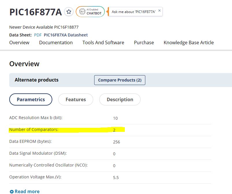
PIC16F87A AI Enabled CHATBOT Ask me about 'PIC16F87A' Newer Device Available PIC16F187 Data Sheet: PDF PIC16F87XA Datasheet Overview Documentation Tools And Software Purchase Knowledge Base Article Overview Alternate products Compare Products (2) Parametrics Features Description ADC Resolution Max b (bit): 10 Number of Comparators: 2 Data EEPROM (bytes): 256 Data Signal Modulator (DSM): 0 Numerically Controlled Oscillator (NCO): 0 Operation Voltage Max.(V): 5.5 Read more
character generator ROM (code 0101) T6963C−0101 is built in as standard. ▯External display memory : 64 KB Max The addresses in display memory of the text area, graphic area and external character generator area are determined by software. ▯Read or Write operations from the CPU do not disturb the display. ▯A
Frequenzen der Einsatze Ais Ergänzungmzu demähbisher angebote nen Frequenzsynthesizerbaustein S 187 bietetSiemens jetztden neuen CMOS- PLL-Baustein TBB 146an. Der TBB 146 unterscheidet sich vom S 187 durch dieunterschiedlicheEinste lung der FrequenzteilerBeim S 187 er folgdiese Einstellunparalleüber
eigentlich kleiner als dort in der Unterschrift steht? Ich komm bei "210"kB nur auf 186, "220" sind 187kB.
Max B. schrieb im Beitrag #8087965: > Also mein Kollege war in Spanien, der hat während der Totalität ca. 2000 > Fotos gemacht und danach in aller Ruhe wieder den Filter aufgesetzt. :) Und hat er
a maximum height of 6 mm and, with the 6-segment collect&place head (S-27 HM), on components to a max. of 8.5 mm. The transport height can be set to allow the machines to be integrated into lines with 830, 900, 930 or 950 mm transport height. Communication between the PCB conveyors of the individual
25 C both polariti1s Q (PNP)2& Q (NPN), unless otherwise noted) G = Pb-Free Package Rating Symbol Max Unit (Note: Microdot may be in either location) Collector-Base Voltage VCBO 50 Vdc *Date Code orientation may vary depending up- on manufacturing location. Collector-Emitter Voltage VCEO 50 Vdc Collector
71015 Einhängekorb PK 2 C Insert basket PK 2 C Panier à accrocher PK 2 C Kunststoff plastic plastique 187 × 90 × 56 mm, L × B × T 187 × 90 × 56 mm, l × w × d 187 × 90 × 56 mm, L × l × P Maschenweite 2 mm mesh size 2 mm largeur de mailles 2 mm Nutzlast max. kg max. load kg charge utile max. kg Bestell-Nr
UART als Dump schickt. Ich habe selbst mal, weil ich zu faul war eine PC-App zu programmieren den MAX7456 OSD Chip so programmiert: Ein PIC16F59 (Baseline-Core, kann fast nichts, hat viele I/Os) hat auf dem Steckbrett ein EPROM (27C128 oder 27C256) ausgelesen und via Bitbang-SPI-Kommandos an den MAX7456 schickte. Das EPROM enthielt den Inhalt des .MCM-Files als konvertierte Binärdaten.
.94 Figure 88: 24-hour HDOP values, in area with with no shadow/obstruction of satellite visibility (max. HDOP < 1.9).......................................95 Figure 89: 24-hour HDOP values, in area with with strong shadow/obstruction of satellite visibility (max. HDOP > 20)............................
Than MAX_FL Bytes and Bad CRC Statistic Register (ENET_RMON_R_JAB)....... 2053 57.5.71 Reserved Statistic Register (ENET_RMON_R_RESVD_0).......................................................................
R910 T 74 53 R1022 T 84 27 R1208 T 183 73 S1204 T 191 74 TP36 B 9 96 TP86 B 179 9 TP137 B 179 54 TP187 B 28 49 R911 T 55 95 R1023 T 107 40 R1209 T 90 92 S1206 T 10 35 TP37 B 24 80 TP87 B 164 17 TP138 B 115 12 TP188 B 23 47 R912 T 79 49 R1024 T 86 37 R1210 T 89 92 TP38 B 18 84 TP88 B 145 14 TP139 B 98
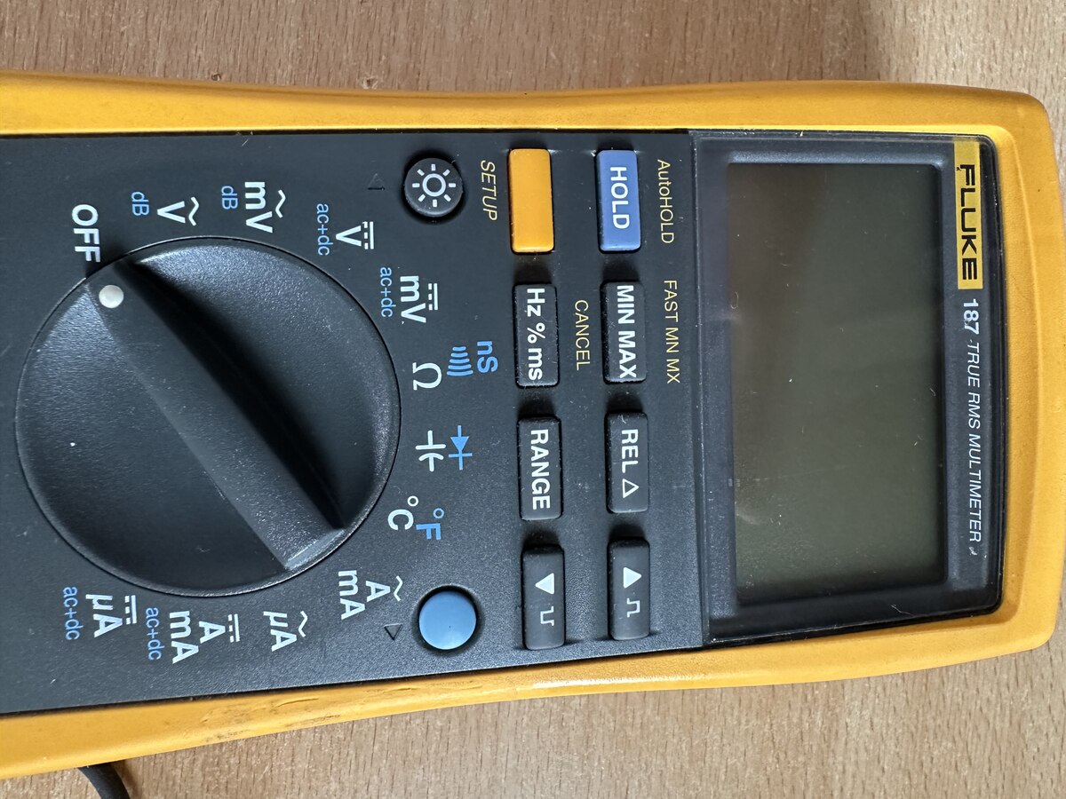
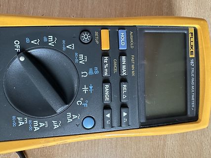
OFF db ~ mV ac+dc V mV ac+dc $\Omega$ ns % ms HOLD AUTOHOLD MIN MAX REL $\Delta$ RANGE $\mu$A ac+dc mA ac+dc $\mu$A ac+dc mA $\sim$ $\text{A}$ $\text{V}$ $\text{C}$ $\text{F}$ $\text{Hz}$ $\text{A}$ FLUKE 187 TRUE RMS MULTIMETER
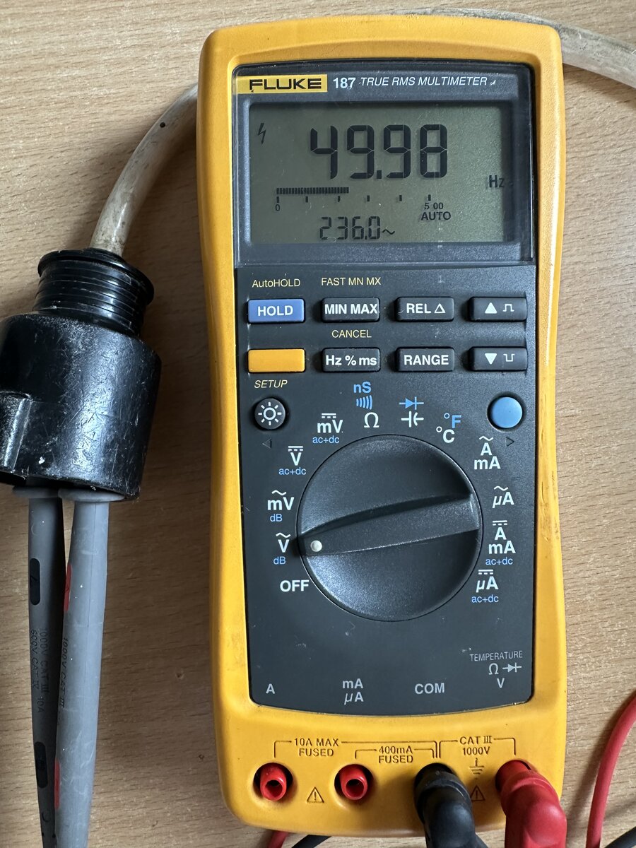
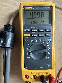
FLUKE 187 TRUE RMS MULTIMETER 49.98 Hz 236.0~ AUTO HOLD MIN MAX REL Hz % ms RANGE SETUP mV Ω °C V mA µA A ac+dc µA ac+dc A ac+dc OFF TEMPERATURE Ω V A mA µA COM 10A MAX FUSED 400mA FUSED CAT III 1000V
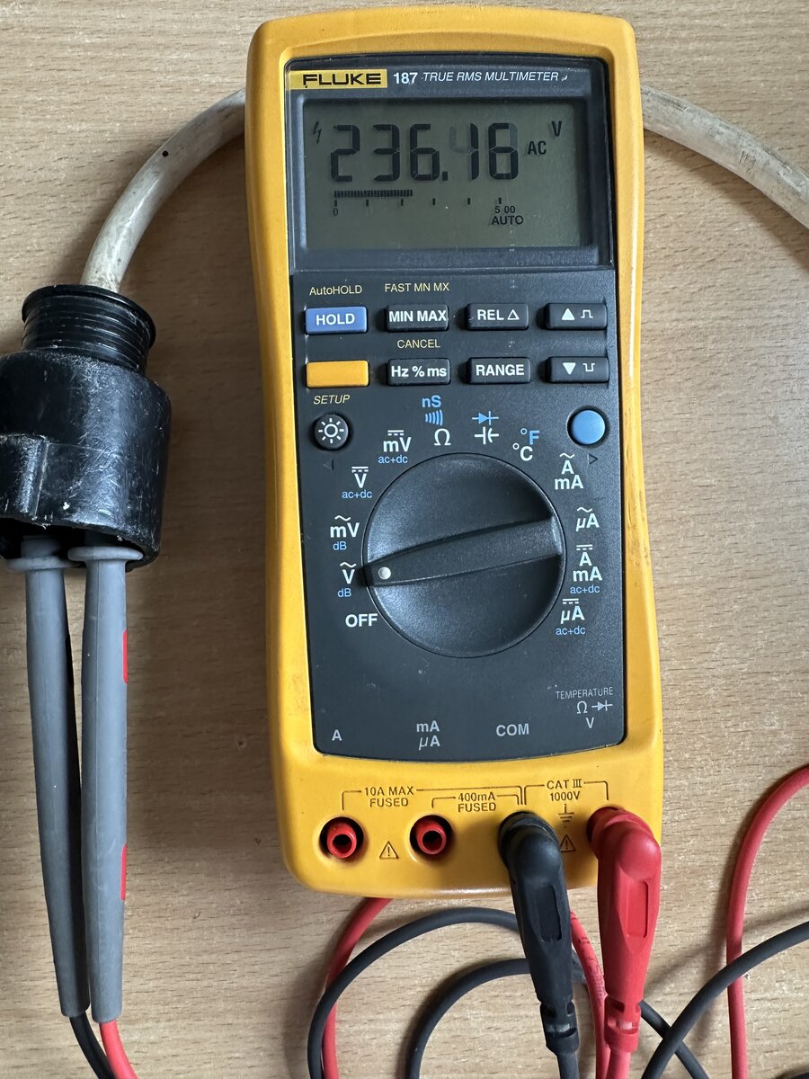
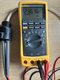
FLUKE 187 TRUE RMS MULTIMETER 236.46 AC 5.00 AUTO HOLD MIN MAX REL Hz % ms RANGE mv ac+dc mv ac+dc dB V ac+dc OFF mA ac+dc µA ac+dc A µA mA µA COM TEMPERATURE Ω + V 10A MAX FUSED 400mA FUSED CAT III 1000V
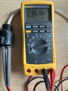
FLUKE 187 TRUE RMS MULTIMETER 236.46 AC 5.00 AUTO HOLD MIN MAX REL Hz % ms RANGE mv ac+dc mv ac+dc dB V ac+dc OFF mA ac+dc µA ac+dc A µA mA µA TEMPERATURE Ω + V COM 10A MAX FUSED 400mA FUSED CAT III 1000V
form C (DPDT) Construction Single Material Gold plate silver tin oxide (AgSnO2) Resistance (initial) Max. 100mOhm at 1A, 6VDC Contact rating 5A, 250VAC / 24VDC Max. carrying current *¹ 7A Max. switching voltage 400VAC/ 300VDC Max. switching power 1,250VA, 120W Min. switching load *² 10mA, 5VDC Life Mechanical
Display p.c.b. 5322 216 91847 532221691847 Das PM2521 verwendet drei LCD-Treiber SAA1062:Seite 56 (54/187) 1.4.6. Display section (Seite 136 (128/187)) Seite 89 (84/187): 5.3. Front Assembly: LCD (L.C. display 5322 130 94033 (532213094033) interconnection rubber 5322 290 84029 (532229084029) Display unit N3 5322 216 74066 (532221674066) Seite 100 (95/187) Figure 57 Display p.c.b. lay-out, conductor side: 59 pins keine der Nummern kommt in der KI-Antwort vor. Das PM2534/PM2535 verwendet das L.C.D. 5322 130 90279 (532213090279) https://manualmachine.com
the counter is full (therefore the counter is also presettable for the DOWN-phase to get a defined max. DOWN-timing in case of a fault). When the DOWN-phase is ready, the contents of the counter is transferred to the output shiftregister and the AZ-phase is started. The timing of the AZ~phase is done
p.c.b. 5322 216 91847 532221691847 Das PM2521 verwendet drei LCD-Treiber SAA1062:Seite 56 (54/187) 1.4.6. Display section (Seite 136 (128/187)) Seite 89 (84/187): 5.3. Front Assembly: LCD (L.C. display 5322 130 94033 (532213094033) interconnection rubber 5322 290 84029 (532229084029) Display unit N3 5322 216 74066 (532221674066) Seite 100 (95/187) Figure 57 Display p.c.b. lay-out, conductor side: 59 pins keine der Nummern kommt in der KI-Antwort vor. Das PM2534/PM2535 verwendet das L.C.D. 5322 130 90279 (532213090279) https://manualmachine.com
measure anode luminous sensitivity) VOLTAGE 0 V ON LIGHT LEVEL OFF 5 6 7 8 9 (minutes) 1 µA ANODE I max. OUTPUT Ii I min. OR Ii I max. I min. 5 6 7 8 9 (minutes) WARM-UP PERIOD (5 minutes or more) THBV4_0440EA Figure 4-40: Light hysteresis In light hysteresis test, the photomultiplier tube is operated
needed in order to keep the junction temperature below the manufacturer’s recommended value, T (J)max Calculate the total theta, θ(°C/W), needed. (T - T ) q JC= (J)max A(max) PD (150 40 ) q JC= 1.4 q JC= 78 ° / W (8) Now choose a device package with a theta at least 10% below this value to account for
Zigbee2Mqtt das Joinen aktiviert. Natürlich ist der Abstand zwischen ESP und Zigbee Stick gering (max. 1m, direkte Sicht). Und falls es irgendwie hilfreich ist: Z2M nutzt den Kanal 11. Ich habe den ESP mehrfach mit idf.py erase-flash flash monitor nach bestem Wissen neu aufgesetzt. Und im Monitor
340084) map I (174) esp_image: segment 3: paddr=0007309c vaddr=408018c4 size=0e474h ( 58484) load I (187) esp_image: segment 4: paddr=00081518 vaddr=4080fd40 size=0233ch ( 9020) load I (194) boot: Loaded app from partition at offset 0x10000 I (194) boot: Disabling RNG early entropy source... I (205
control and could cause personal injury or NOTE: property damage. 1. All leads 8" long minimum. D D MAX. MAX. 2 H MAX. H R z 2 MW MAX. O X 6 1 1 W C X R5 MAX. N P P7 T 1 S .188 ± .015 DIA. (2 HOLES) STYLE A 1 3 MD MW W MAX. PRIMARY SECONDARY 117V, 50/60 Hz 4 24V CT MS (4 PLACES) STYLE NV 2 5 SCHEMATIC
H2 I H 1 L 0 - 40 0 55 85 125 150 P d Tamb(°C) Note • Zero power is considered as measuring power max. 1 % of max. power. PHYSICAL DIMENSIONS FOR RELEVANT TYPE (all dimensions in millimeters) H1 R25VALUE BMAX. d H2 MAX. L P T MAX. MIN. MAX. 3.3 to 220 5.0 0.6 ± 0.06 1.0 4.0 6.0 24 ± 1.5 2.54 4.0
Schaltung? Die sieht mir doch ziemlich weltfremd aus. Sieht nach Kainka aus. Schätzt man mal die max Ausgangsspannung sehr wohlwollend mit 8Veff ab so errechnen sich an 10kOhm Anodenwiderstand max 6,4mW Ausgangsleistung. Ist preisverdächtig für den ineffizientesten Verstärker auf diesem Planeten.
H2 I H 1 L 0 - 40 0 55 85 125 150 P d Tamb(°C) Note • Zero power is considered as measuring power max. 1 % of max. power. PHYSICAL DIMENSIONS FOR RELEVANT TYPE (all dimensions in millimeters) H1 R25VALUE BMAX. d H2 MAX. L P T MAX. MIN. MAX. 3.3 to 220 5.0 0.6 ± 0.06 1.0 4.0 6.0 24 ± 1.5 2.54 4.0
hochgenaue Widerstände“ verwendet wurden. Neben drei Luftrimmern gibt es noch zwei Trimmpotentiometer (R187 und R189), die für Effektivwert (RMS) und Spitzenwert (Peak) zuständig sind und sich in der Nähe des Drehspulinstruments befinden. Ich habe mal einige einfache Tests mit einem 1-kHz-Sinus und verschiedenen
immer in der Stellung „RMS eff.“. Ich gehe daher davon aus, dass ein Eingriff an den Trimmern R187/R189 keinen Sinn ergibt, da eine Veränderung hier auch die bislang genauen Messbereiche beeinflussen würde. Meine Frage: Können solche Ungenauigkeiten (zu hohe Anzeigewerte) durch gealterte Kondensatoren
0.25) / 2.750 (± 0.010) Length (mm/in) 100.35 (+0.20/-0.25) / 3.951 (+0.008/-0.010) Weight (g/lb) max 90 / 0.198 85 / 0.187 Average latency 5.6 ms Startup current, Max (+5V) 1.0 A Voltage tolerance (including noise) 5V ± 5% Non-Operating (Ambient °C) –40° to 70° Operating ambient temperature (min °C) 0° Operating temperature (drive case max °C) 60° † 20°C per hour max (operating) Temperature gradient 35°C per hour max (non-operating) Relative humidity 5% to 95% (operating) 5% to 95% (non-operating) Relative humidity gradient (max) 30%
RatedvoltagerangeU 16…450V a • RoHS compliant n SurgevoltageU U ≤315V:U =1,15U ;U >315V:U =1,10U c S R S R R S R n Max.reversevoltage 2V • REACH compliant t m o Categorytemperaturerange -40°C...+85°C i n LeakagecurrentI afLer5min@U R ≤0,008*C [µFR*U [V]+6RA[µA] , c Usefullife3000h @85°C;U ;I R R Requirements o ΔC/C≤
RatedvoltagerangeU 16…450V a • RoHS compliant n SurgevoltageU U ≤315V:U =1,15U ;U >315V:U =1,10U c S R S R R S R n Max.reversevoltage 2V • REACH compliant t m o Categorytemperaturerange -40°C...+85°C i n LeakagecurrentI afLer5min@U R ≤0,008*C [µFR*U [V]+6RA[µA] , c Usefullife3000h @85°C;U ;I R R Requirements o ΔC/C≤
specifications are atAT =2℃, VCC =5V,unless otherwise noted. UNI SYMBOL PARAMETER CONDITIONS MIN TYP MAX TS VCC Input Supply Voltage ● 4.0 5 9.0 V Input Supply Current Charge Mode, RPROG= 10k ● 150 500 µA StandbyMode(Charge ● 45 100 µA I Terminated) ● 45 100 µA CC Shutdown Mode (RPROGNot 45 100 Connected
esp_system_init_fn_init_show_app_info at C:/Users/localuser/esp/v5.5.1/esp-idf/components/esp_app_format/esp_app_desc.c:123 I (187) app_init: Application information: I (190) app_init: Project name: sleep-test I (194) app_init: App version: 1 I (198) app_init: Compile time: Dec 27 2025 14:11:52 I (203) app_init
/efuse/src/esp_efuse_startup.c:47 I (217) efuse_init: Min chip rev: v0.0 I (220) efuse_init: Max chip rev: v1.99 I (224) efuse_init: Chip rev: v0.1 D (228) cpu_start: calling init function: 0x42003422 on core: 0 --- 0x42003422: __esp_system_init_fn_init_heap at C:/Users/localuser
It will take one MCU instruction cycle to calculate. CRC-16-IBM (Modbus) Polynomial representation: 187h Bit 7 Bit 6 Bit 5 Bit 4 Bit 3 Bit 2 Bit 1 Bit 0 CRCDL CRCDL R/W R/W Reset 1 1 1 1 1 1 1 1 187h.7~0 CRCDL: 16-bit CRC checksum data bit 7~0 188h Bit 7 Bit 6 Bit 5 Bit 4 Bit 3 Bit 2 Bit 1 Bit 0 CRCDH
It will take one MCU instruction cycle to calculate. CRC-16-IBM (Modbus) Polynomial representation: 187h Bit 7 Bit 6 Bit 5 Bit 4 Bit 3 Bit 2 Bit 1 Bit 0 CRCDL CRCDL R/W R/W Reset 1 1 1 1 1 1 1 1 187h.7~0 CRCDL: 16-bit CRC checksum data bit 7~0 188h Bit 7 Bit 6 Bit 5 Bit 4 Bit 3 Bit 2 Bit 1 Bit 0 CRCDH
and V ds being the intrinsic drain-source voltage. The charge and capacitances are: for V > V new max 168 V max Vnew − V max Q gs = Cgs0· 2·Vbi 1 − 1 − + (11.364) V bi 1 − VVax bi ∂Q gs C gs0 ∂Vnew = · (11.365) ∂Vgs 1 − VVax ∂V gs bi ∂Q gs C gs0 ∂Vnew = · (11.366) ∂Vgd 1 − VVax ∂V gd bi and
Hat nichts mit reich zu tun, sondern mit dem Tuning. Der Motor braucht die höhere Oktanzugabe. Max. und nur zur Not, da kann ich Superplus tanken. So hat jeder seine Hobbys. Der eine hat ein Wohnmobil, der andere ein Segelboot und ich habe eben schnelle Fahrzeuge.

 Bild
Bild

 Bild
Bild
 Bild
Bild
 Bild
Bild
 Bild
Bild
 Bild
Bild
 Bild
Bild
 Bild
Bild