es auch für andere Controller was. Siemens S55/C60. S55-Display Pinbelegung Forumbeitrag Siemens S65/M65/CX65. S65-Display vom Siemens S65/M65/CX65, 132x176 Pixel, 65536 Farben, günstig als Ersatzteil zu bekommen. Nokia 3210/3310. Bibliothek für Nokia 3310 Lcd Ansteuerung in "C" von - sehr gut (aktualisiert
Dokumentation siehe unter Downloads. Das PS/2 Maus und PS/2- oder AT-Tastatur-Protokoll (Original auf * S.N.A.P - Scaleable Node Address Protocol. S.N.A.P is an free and open network protocol. The protocol was primary developed for PLM-24 based home automation and control systems but it is a generic protocol
) { count = maxlen; } if (count) { P = (UMEM_WIDTH*) EPControlRxBuffer; n = 2; i = count; D = *P++; while (i > 0) { *PBuffer = D & 0xFF; D = D >> 8; --n; if (!n) { D = *P++; n = 2; } --i; ++PBuffer; } } ClearBuffer(logEpCtrl); return count; } int WriteControlBlock
N. M. schrieb im Beitrag #8090001: > Der Hans scheint dagegen riesig Ahnung zu haben. Habe ich nicht behauptet. Die Praxis zeigt mir aber das das funktioniert. N. M. schrieb im Beitrag #8090001:
sondern kommt von _VDD_ vom Mikrocontroller. Ich habe meine Schemazeichnung mal aktualisiert. _RX_, _TX_ und _GND_ waren schon klar, die Ausgänge habe ich mit den richtigen Pins der Klemmleiste verbunden. Am meisten Sinn ergeben würde es, wenn der _SWIM_-Pin sowohl mit _nRE_ als auch _DE_ verbunden
sog. Bunkerkondensator, der bei digitalen Schaltungen an jedem Digitalbaustein Standard und eher 100nF groß ist. (bei SMD-Keramikkondensatoren steht dann 104 für 100nF drauf; 105 wären 1µF).
100μV maximum ► Offset voltage drift: 1.5μV/°C maximum ► MSL1 rated ► Low-input bias current: 1.5nA maximum ► Low-voltage noise density: 6.9nV/√Hz typical at f = 1kHz ► CMRR, PSRR, and AV > 120dB minimum ► Low supply current: 400μA per amplifier typical ► Gain bandwidth product: 3.6MHz ► Dual-supply
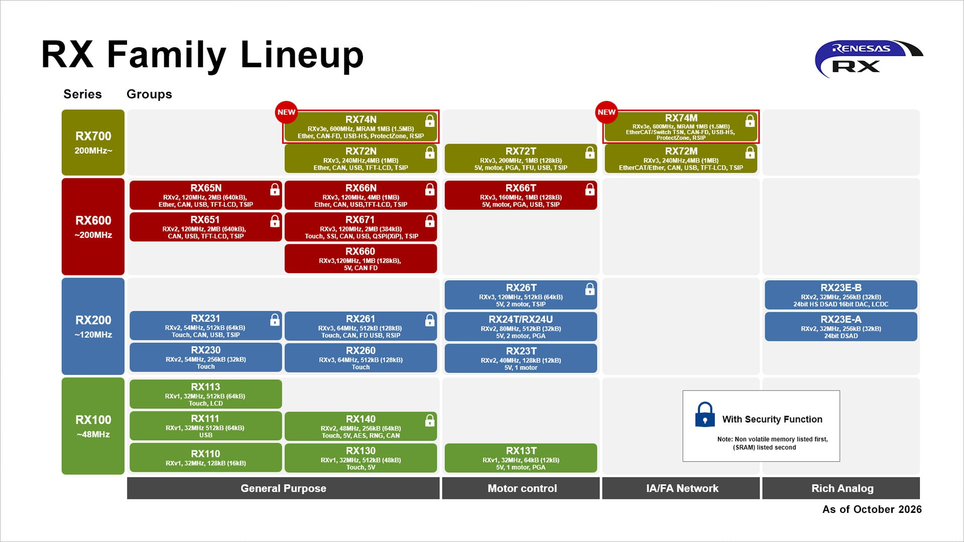
attachment/702553/23.png) Bildquelle: NXP ### Kinetic Technologies KTS1625 – I2C-Expander für 1.65 bis 5.5V Wer einen mit sechzehn GPIO-Pins ausgestatteten GPIO-Expander sucht, kann nun auch bei Kinetic einkaufen. Zu beachten ist, dass er nur in einem WQFN-Gehäuse erhältlich ist. ### Renesas RX14T
natürlich Keil8051 (teuer). Ach ja, und mir fehlt die passende Anwendung für die alten Dinger. Habe noch 65 Stck. At89C52ED2, die waren mir vor 15 Jahren Gold wert aber heute?
Bernd N. schrieb im Beitrag #8083161: > Keil ist kostenlos zu haben. Ja, aber so weit ich weiß, nur bis 1kB Objektdateigröße, oder hat sich daran etwas geändert? Mit der IDE habe ich richtig gerne gearbeitet
the AC power in Zone 2/Class I, Div. 2 Hazardous Areas/Locations) Brown (live (L)) Blue (neutral (N)) Yellow/green (grounding conductor) Hook up the scale to the power supply in conformance with the installation requirements of your country. 1–24 The IP 65-protected ING-2 no. 69 71899 AC adapter is
118183B268A Note: All resistors ±1% 10BASET External Components and Hookup Am79C961 1583 AMD P R E L I M I N A R Y ABSOLUTE MAXIMUM RATINGS OPERATING RANGES Storage Temperature . . . . . . . . . . . –65°C to +150°C Commercial (C) Devices Ambient Temperature Temperature (T A) . . . . . . . . . . . . . . 0°C
13, speziell 13.2, das ist dort schon die > Minimalbeschaltung. Woher weißt du, was auf dem SN65HVD230_CAN_Modul alles drauf ist? Im Datenblatt des SN65HVD230 CAN-Transceivers geht es in Kap. 13 um das Layout. https://www.ti.com/lit/ds/symlink/sn65hvd230.pdf
nur zwei zusätzliche Widerstände und nicht mal ein 100n Kondesator, gruselig.... > Im Datenblatt des SN65HVD230 CAN-Transceivers geht es in Kap. 13 um das > Layout. > https://www.ti.com/lit/ds/symlink/sn65hvd230.pdf Ja, sag ich doch. Einen "typical
Wahrscheinlich könnte man mit llama.cpp Einfluss nehmen. In dem Video wird auf die Parameter wie "--n-gpu-layers" eingegangen, um die Verteilung der Rechenleistung etwas zu steuern. https://www.youtube.com/watch?v=8F_5pdcD3HY
ich natuerlich auch schon gemacht. Klar ist schneller. Denke gerade darueber nach 400Euro fuer eine RX9060 mit 16Gig rauszuhauen. In dem Zusammenhang mal einen Tip. Ich habe aktuell eine 7-8Jahre alte RX550 mit 8GB Vram. Mein Rechner lief immer bombenstabil! Aber mit den KIs ist er gerne mal voll brutal
VBR VBL POWER BRIDGE OUTR ROM/OTP/EPROM 16K OUTL A PGND D RAM 256B R E TEMPSENSOR S EEPROM 128B S N D AD2 D 10-bit ADC AD3 WATCHDOG A A AD4 B CONTROLLER U PWM 1 S RX TX PWM 2 CAN_H CAN CAN_L TRANSCEIVER PWMO PWMO PWMI PWMI PORT B PB0 -> PB1 TIMER 2 PORT A TIMER 1 PA0 -> PA7 9/125 General description
voltage on LIN externally forced; LIN slope time <500 ns; CRXD = 20 pF; R = 2.4 k ; (see RXD Fig.5) PropRxDom − PropRxRec f(slope)(dom) fall time LIN normal slope mode; − 16 27 s (100% to 0%) CL= 10 nF; R L 500 ; V = 12 V; transition BAT from recessive to dominant; note 4 (see Fig.5) r(slope)(rec) rise time
coordinates. x R N h cos cos λ (20a) y R N h cos sin λ (21a) 2 z R N 1 e h sin (22a) 2.4 Planar regional coordinates, projection Usually the ordnance survey depicts the position
FEBRUARY 2026 5 Pin Configuration and Functions 5.1 Pin Diagram Figure 5-1 shows pin assignments for the 65-pin LGA package. S L W R _ F P L n G G G G G O G G G P K e G D D D D D U D D D N N e D T t GND 29 28 27 26 25 24 23 22 21 20 19 18 17 16 15 GND GND 30 14 GND SWCLK GND 31 13 GND 32 12 SWDIO GND 33 11
~ > 3 2 2 2. N oO ro) oO oO i ( 65 , 3.2. A C R A N G E S ‘ n =2) a == > > 5 a & z & & oy 2 2 2y 2 a. = a a fn) Qa my Ss \ T 2 > Ry 2 2 . ~ m oid S os ) a) oO - a Si] + +o 8 +1 g +! SQ >E E 1 ao oO ro) et) OQ i) Oo
feedsthe current multipliers, togivethe currents Irxshown inthe table,depending on the selected signal R N G A, R N G B and R N G C. As stated,the voltageVx developed across Rx isapplied tothe ADC formeasurements. However, the ADC input resistance isfinite (10 MQ) and thesmall inputcurrentdrawn by the ADC
is stopped only E n1 n2 n3 by commands (e.g. receipt or touch macros) ESC M Automatic macros cyclically A n1 n2 n3 Automatically run macros n1 to n2 cyclically; n3 = pause in 1/10s. Execution is stopped by commands (e.g
) 0x0011 (Sn_DPORT1) 0x0025 (Sn_TX_WR0) 0x0001 (Sn_TX_WR1) Socket n Socket n RX Received Socket n Interrupt Maximum Segment Size 0x0026 Size 0x0002 (Sn_IR) 0x0012 (Sn_MSSR0) 0x0027 (Sn_RX_RSR0) 0x0013 (Sn_MSSR1) (Sn_RX_RSR1) Socket n Status Socket n RX Read Pointer 0x0003 (Sn_SR) 0x0014 Reserved 0x0028 (Sn_RX_RD0) Socket n Source Port Socket n IP TOS 0x0029 (Sn_RX_RD1) 0x0004 (Sn_PORT0) 0x0015 (Sn_TOS) Socket n RX Write 0x0005 (Sn_PORT1) Socket n IP TTL 0x002A Pointer Socket n Destination 0x0016 (Sn_TTL)
n TCER- ENI L- U r T e s B B - - e u r u l e h g - X X X t n s n h ENI L- NO Ü S r T R T R S p e A c s v S e f N F t TXE- FFO O O N TXE- NO l t - g l t S s r - n D e i i r / es t a L n e n a n T N i A
zusammen gelötet. Ein Kupferring mit 70cm Durchmesser fertig gemacht. Das Modul mit 9V Akku in eine IP65 Dose erstmal eingebaut. Als Antennenkabel ein 5 Meter RG58 angelötet an den Antennenausgang. Bin jetzt am Wochenende dazu gekommen die Antenne mal gegen ein 10 Meter Langdraht und eine Mini Whip RX
x x x x x N+25 . N+2 x x x x x x N+10 x x x x x N+18 x x x x x N+26 . N+3 x x x x x x N+ll x x x x x N+19 x x x x x N+27 . N+4 x x x x x x N+12 x x x x x N+20 x x x x x N+28 . N+5 x x x x x x N+13 x x x x x N+21 x x x x x N+29 . N+6 x x x x x x N+14 x x x x x N+22 x x x x x N+30 . N+7 x x x x x x N+15 x x x x x N+23 x x x x x N+31 . N+768 x x x x x N+776 x x x x x N+784 x x x x x N+792 N+769 x x x x x N+777 x x x x x N+
#8013593: > Guten Abend liebes Forum, > ich habe eine Frage: ich möchte einen ESP32 (mit 3,3Volt) via RX / TX > mit > einem 8051 (mit 5Volt) verbinden .. > Ich habe die Schaltung im Web gefunden. Sie hat einen 6N137 an Board. AUA! DU braucht einen EINFACHEN [[Pegelwandler]]. > eine eigene Masse
Stefan S. schrieb im Beitrag #8013593: > ich möchte einen ESP32 (mit 3,3Volt) via RX / TX > mit einem 8051 (mit 5Volt) verbinden .. > Wie am besten? 3,3 -> 5 mit HCT oder AHCT Gatter. 5 -> 3,3 mit LVC oder VHC Gatter. Es gibt auch interessante IC (zwar in TSSOP-14, 0,65 mm Raster
English - www.onlinedoctranslator.com 1 2 3 4 5 6 SWD and USART1 interfaces A A P1 SWCLK PA14 USART1-RX PA10 Here, the STM32H723 is divided into two parts, but they are actually the same chip. 1 5 L1 SWDIO PA13 2 6 USART1-TX PA9 CBG160808U121T Ferrite beads/120200mAMHz GND 3 7 R7 1KRST VDDA 3.3V Analog
DocID026915 Rev 1 5/19 19 Differential configuration AN4586 Figure 3. Differential configuration example ▯▯▯N 5I▯ ▯▯N 9▯▯ ▯▯▯9 5J▯ 9LR 5J▯ 5I▯ 9▯▯ ▯▯▯9 ▯▯N ▯▯▯N In Figure 3, the Vicm of the op amp is 9 V. Thus, if the op amp is supplied by 5 V, we cannot measure the voltage difference. We may even damage the
100MbpsFastEthernetPhysicalLayer TX/FXSingleChipTransceiver 4. Pin Configuration: DM9161 LQFP E S B 1 N E [ [ [ [ [ M D D D D D R Y Y Y Y I A C # H H H H M H / R ] P]P ] ] / / L D N N D [ [ [ [ O L S C N D E D D D D D D C C R D M R D R R R R MX X X 6 5 4 3 2 1 0 9 8 7 6 5 3 3 3 3 3 3 3 2 2 2 2 2 RXDV/TESTMODE

 Bild
Bild
 Bild
Bild