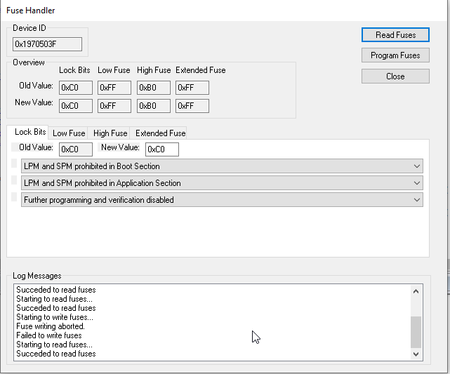
ATmega1284p: Spontane Änderung von lock bits

OP #6312282
Lesenswert?

Hallo,

ich habe auf einem 1284p einen Bootloader, der AES256-verschlüsselte 
Firmware flasht. Dabei ist BOOTRST und JTAG auf on, On-Chip Debug 
Enabled und ISP sind deaktiviert.
Damit nichts mehr ausgelesen werden kann, stelle ich

"LPM and SPM prohibited in Boot Section"
"No lock on SPM and LPM in Application Section"
"Further programming and verification disabled"

ein.
Das funktioniert auch alles und die Firmare läuft. Mehrere Geräte werden 
aktiv in Messanordnungen eingesetzt. Allerdings bekomme ich ein mal im 
halben Jahr ein Gerät zurück, welches den Bootloader zwar startet, 
dieser aber bei der CRC-Prüfung der Firmware einen Fehler ausspuckt. 
Wenn ich die lock bits auslese, dann steht da

"LPM and SPM prohibited in Boot Section"
LPM and SPM prohibited in Application Section
"Further programming and verification disabled"

Wie ist das möglich? Ich hätte die lock bits so gar nicht setzen können, 
denn dann kann man die Firmware gar nicht mehr flashen und das Gerät 
hätte gar nicht funktioniert. D.h. im Einsatz haben sich die lock bits 
verändert, oder?
Angehängte Dateien:
#6312291
Lesenswert?

Die Lockbits können vom Bootloader aus gesetzt werden.
Ist das BOR enabled?

"Flash corruption can easily be avoided by following these design 
recommendations (one is sufficient):
1. If there is no need for a Boot Loader update in the system, program 
the Boot Loader Lock bits to prevent any Boot Loader software updates.
2. Keep the AVR RESET active (low) during periods of insufficient power 
supply voltage. This can be done by enabling the internal Brown-out 
Detector (BOD) if the operating voltage matches the detection level. If 
not, an external low VCC reset protection circuit can be used. If a 
reset occurs while a write operation is in progress, the write operation 
will be completed provided that the power supply voltage is sufficient.
3. Keep the AVR core in Power-down sleep mode during periods of low VCC. 
This will prevent the CPU from attempting to decode and execute 
instructions, effectively protecting the SPMCSR Register and thus the 
Flash from unintentional writes."
OP #6312337
Lesenswert?

Super, danke!
Diese Problematik war mir gar nicht bewusst. Ich merke auch, dass der 
Eingangskondensator relativ groß ist. Nach Strom-Aus dauert es knapp 2 
Sekunden, bis LCD erlischt. D.h. der Spannungsabfall dauert relatv 
lange. Vielleicht liegt es wirklich daran.
Werde nun BOD aktivieren, mal sehen ob es hilft)

Antwort schreiben

Bitte melde dich an, um einen Beitrag zu schreiben.

oder

Mit Google-Account einloggen

Die Registrierung ist kostenlos und dauert nur eine Minute.

Jetzt registrieren