auch ein interessantes Video zu der Thematik veröffentlicht: https://www.youtube.com/watch?v=3FDXuE8TcXI
Solch ein Einzelgatter zur Taktauffrischung benötigt doch "keinen" Platz mehr. Beispiel: das SN74AUC1G17 im DSBGA-Gehäuse ist doch schon fast als Feinstaub zu bezeichnen. Und mit maximal 1,9 ns @1,8V und 15 pF Last ist es fünfmal so schnell wie das 74LVC1G11.
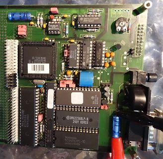
ist einiges komplexer als Laien denken. Im Gegenteil. Das Teil ist sogar ziemlich einfach: Am TC9242 sitzt ein Quarz. Dessen Frequenz wird in dem Baustein geteilt und am Pin CPOUT ausgegeben. Dieser Takt wird im CPLD weiter geteilt in den 4046 (PLL) gegeben und mit der ebenfalls vom CPLD geteilten VCO-Frequenz verglichen. Das Ergebnis, eine digital variable Frequenz, wird zurück zum TC9242 gegeben, der diese Frequenz (nach weiterem teilen) mit dem Frequenzgenerator des Motors vergleicht und daraus eine Regelspannung für den BLDC-Treiber TA7259 erzeugt. That's it. Der Prozessor muss
Erdrotation ist mindestens quarzgenau, da rentiert sich die Schaltung. Hier die Beschaltung eines (74HC)40103 als Teiler durch N. Den 40103 gibt es in der alten langsameren CMOS-Version und der schnelleren HC-MOS, hier das Datenblatt von Philips zum 74HC40103: https://assets.nexperia.com/documents/data-sheet/74HC40103.pdf Achtung, die HC-MOS geht nur bis max. 6V Betriebsspannung, die alte bis >15V. CP clock-pulse ist der Eingang vom Quarzoszillator kommend, /TC und /PE verbunden sind der Ausgang, /PL und
Framework: Arduino Gegeben ist: - Arduino mit ATmega328p Prozessor - Schieberegistermodul mit SN74HC595 und 8 Leuchtdioden - 10 KOhm Potenziometer - Library "sn74hc595" Viel Erfolg und Spaß beim Tüfteln
Framework: Arduino Gegeben ist: - Arduino mit ATmega328p Prozessor - Schieberegistermodul mit SN74HC595 und 8 Leuchtdioden - 10 KOhm Potenziometer - Library "sn74hc595" Viel Erfolg und Spaß beim Tüfteln
a non-saturating Schottky Number of inputs depends on the gate. clamped transistor technique. The 74SOO GENERAL TTL CIRCUIT family of TIL products are very high parlor, mance, high power devices. The most popu CHARACTERISTICS lar TIL category is the 74LS Low Power All TIL products are derived from a
, 4.19, 4.91, 5.00, 6.00, 8.00, 10.00MHz) *2 At -20 to +80D *3 For 10 years at room temperature *4 TC74HCU04 is used as the standard circuit for the MXJ040 series. *5 If connected with incorrect orientation, the above specification may not be guaranteed. *6 CSTCS series shall be recommended in automotive
in Zahlung geben können, bei gleichzeitiger Abnahme einer A77 Viertelspurmaschine, plus einer Sony TC377 Maschine. > Und unter der rechten Bandmaschine steht eine d&b audiotechnik P1200A > Endstufe? Darunter ein Stereo-Graficequalizer vom Typ Fisher EQ-273? > Plattenspieler auch von Fisher? Richtig
erörtert. Wenn, dann nimm lieber den TL084. Beide haben die selben hochohmigen J-FET Eingänge. Der 74 ist der LowPower Nachfolger. Der 84 lässt aber erwarten, das er geringfügig rauschärmer sein sollte, da er intern etwas niederohmiger ist. Deshalb verbraucht er ja etwas mehr Strom.
, units with a negative TC may cycle between overrange FIGURE 4B. and a non-overrange count as the die alternately heats and cools. All these problems are of course eliminated if an external FIGURE 4. USING AN EXTERNAL REFERENCE
mobile radio sets. RoHS COMPLIANT RD70HVF1C-501 is a RoHS compliant products. ABSOLUTE MAXIMUM RATINGS (Tc=25 °C UNLESS OTHERWISE NOTED) SYMBOL PARAMETER CONDITIONS RATINGS UNIT V DSS Drain to source voltage Vgs=0V 30 V V GSS Gate to source voltage Vds=0V -5/+10 V Pch Channel dissipation Tc=25 °C 150 W Pin
I-U-Kennlinienschreiber. Digitale Bausteine werden zusammen mit dem analogen Teil berechnet: Gatter, Flipflops, Zähler, 74HC595. Arduino Uno, Nano und Mega mit echtem .hex-Programm, dazu Module: LCD 16×2 (auch über I2C), I2C-EEPROM, DHT11/DHT22, HC-SR04, Servo. Ein Sketch aus dem Programmfenster landet mit einem Befehl
PWL (auch aus CSV), PRBS und Rauschen. Neue SPICE-Elemente und Optionen: Temperaturkoeffizienten TC1/TC2 für Widerstände; Thyristor und Triac, Relais, Leitung; .LIB und .INCLUDE. Analysebericht als HTML, Zweiton-Intermodulation (IMD) und Wirkungsgrad, Diagramm in Datei, Signal aus CSV, Cursor mit
TSM Peak gate current GRM 0.5 A Average gate power P 0.3 W G(av) Operating case temperature range TC -5 to +85 °C Storage temperature range T -10 to +110 °C stg Lead temperature during soldering 1.6 mm from the case for 10 seconds Tlead 230 °C electrical characteristics at 25°C case temperature (unless
5 VDC and T MINT AT MAX unless otherwise specified. Symbol Parameter Conditions Min Typ Max Units TC Conversion Time CLK= 640 kHz (Note 6) 103 114 µs TC Conversion Time (Notes 5, 6) 66 73 1/CLK fCLK Clock Frequency VCC= 5V, (Note 5) 100 640 1460 kHz Clock Duty Cycle 40 60 % CR Conversion Rate in Free-Running
tissaious'sdFigur zun9.nisse ist ein sauberer Koplspiegel Vorausset- AIs w)eß9eräte uerden empfohlen: Tongenerator TC 40 . lvli-IlivoltmeterIvlV0 0szilLoskop z. B. G0 15 MSI Stromaufnahme Kontokt 6 Die Stromaufnahme beträgt bei ei.ngelegter Cassette am Bandanfang: \ bei Uiedergabe ohne 5igna1, max. 25 mA bei Aufnahme
A NONE No Need WBPPGM V5.08 NATIONAL BPROM DM54S573/A/B NONE No Need WBPPGM V5.08 NATIONAL BPROM DM74LS471 NONE No Need WBPPGM V5.08 NATIONAL BPROM DM74S188 NONE No Need WBPPGM V5.08 NATIONAL BPROM DM74S287 NONE No Need WBPPGM V5.08 NATIONAL BPROM DM74S288 NONE No Need WBPPGM V5.08 NATIONAL BPROM DM74S387
GSto 10 V Switching charge Q sw - 20 - nC VDD50 V, I D30 A, V =GSto 10 V Gate charge total Q g - 56 74 nC VDD50 V, I D30 A, V =GSto 10 V Gate plateau voltage Vplateau - 4.2 - V VDD50 V, I D30 A, V =GSto 10 V Output charge Q oss - 73 97 - VDD50 V, V =GSV 1) See ″Gate charge waveforms″ for parameter definition
(Continued) SUPPLY A TEST PARAMETER SYMBOL CONDITIONS MIN TYP MAX UNITS o Temperature Coefficient TC - 40 - ppm/ C Supply Voltage (V++ -V-) VSUPPLY ±10 - ±16 V Supply Current Total SUPPLY - 6 14 mA NOTES: o 8. The input bias currents are junction leakage currents which approximately double for every
74 52 D903 T 71 57 L803 T 17 71 R209 B 82 61 R625 T 43 27 C314 B 127 49 C702 T 168 20 C838 T 29 72 C1000 T 101 31 L804 T 74 73 R210 B 99 73 R626 T 49 21 D904 T 65 106 C315 B 131 58 C703 T 175 24 C839 T
Input unit eee eee eee e e e e e e h h 6-3 6.2.4 Interchanging input unit .......eeeeeeeecereeeeecee O74 6.2.5 Fuses Pe eeeeee ee 6-4 6.3 Trouble shooting e e e e 6-5 7. SAFETY INSPECTION AND TESTS AFTER REPAIR AND MAINTENANCE IN THE PRIMARY CIRCUIT 7-1 7.1 General directives 2.2.02 ceecsccceccesecceseseseens
...................................................................................................74 21.1 Avoid leakage current in POWER-OFF mode ...................................................................................................................74 21.2 LED output configuration.......
ident corrected 65 – Description of t corrected LLIV 65 – Program Memory Read Cycle: t PXAV added 74 – Oscillator circuit drawings: MQFP-100-2 pin numbers added. Page Subjects (changes since last revision 01.94) – Minor changes on several pages 47 – Table 6 corrected Semiconductor Group 2 1994-05-01
B MTP8N50E 0.98 (with MC33262based PFC) Of course, the sicannot be zero, but it is small enough to TC= 40°C (steady state, in free air) make this new technology a good choice to design an electronic lamp ballast. The time delays built with R3/Ciss , R4/Ciss and Q1 Q2 Also, the ON voltage is very close
sal Count r e Gate & ExtArm j ≡ M M MEASURE » ⅛ ⅛ ⅛ z l irι ,3 GATE:TIME RUN j⅞jjkJg 4tW ≡ RUN jGΛT⅛TC> j-⅜ ⅛ ..H... START: fS ii≡ iΠ H i ≡* ¾ a ⅛ ⅝ ι⅛ r⅛ ⅞ﮏa⅝⅛⅛π⅛M s ∞ STOP: s ≈ ----------<__------', w ⅜wΓ" 'jooi------ ¾ B ≡ rτS ∣Gλ⅛r'0⁄G⁄TS'''⅝j ExtArm ?: IOf ⅜ ≡ HP 5315 31A/132A/132A Universa Count
This measurement should be 74.2 mm for the S-27 HM TIP Move one PCB into the placement area and clamp the PCB in place. Now measure the distance between the top edge of the lifting table (rubber stop) and the bottom edge of the PCB. This height should be exactly 94 mm for the HS-60 and 74 mm for the S-27 HM. NOTE The actuator underthe clampingsensormust bemounted0.2 -0.3 mm lowerto guarantee reliable actuation of the clamping sensor. Æ Push one PCB manually through the entire PCB conveyor
500 1000 1500 2000 I Q E SUPPLY VOLTAGE (V) THBV4_0445EA Figure 4-45: Example of EADCI THBV4_0445EA 74 CHAPTER 4 CHARACTERISTICS OF PHOTOMULTIPLIER TUBES b) AC expression In low-level-light measurements, the DC components of dark current can be subtracted. The lower limit of light detection is determined

 Bild
 Bild
 Bild

 Bild

 Bild