Machine Model 25 V (Note: Microdot may be in either location) THERMAL RESISTANCE RATINGS Rating Symbol Max Unit ORDERING INFORMATION Junction−to−Ambient – Steady State (Note 1) RqJA 450 °C/W Device Package Shipping† Junction−to−Ambient − t v 5 s (Note 1) R 375 qJA NTS4409NT1G SOT−323 3000 / Tape & Reel Stresses
nicht als "Aus" sondern als Detonator. Nur wusste das keiner der Ingenieure vor Ort bevor man es 01:23:40 mit dem bekannten katastrophalen Ausgang testete . https://de.wikipedia.org/wiki/Nuklearkatastrophe_von_Tschernobyl#Ursachen
Max I. schrieb im Beitrag #7859678: > Drucktaste Der Name ist nicht wichtig, aber die Funktion. Es es ein einrastender Taster mit Rückstellsicherung.
(aber nicht ideal). Der Max40200 ist relativ teuer mit 50-60Cent.. x2 sind es schon 1,20. Passende High-Side Switches gibts viele, auch günstig vom Chinesen zB CH217K (15Cent). Funktionieren denn meine angedachten Lösungen
das zu lösen oder alternative interessante Bauteile? So was wie einen 2kanaligen PowerMuxer im SOT23 oder so..
L6203 needs a suit- able cooling. By using two squarecopper sidesin a similar way as it shown in Fig. 23, Fig. 21 indicates how to choose the on board heatsink area when the L6201 totalpower dissipation is known since: Figurre23: TypicalR Th J-ambvs. Two ”On Board” RTh j-amb (Tj max.– Tamb max) / tot SquareHeatsink
2,85V sein und der GPIO ist möglicherweise je nach verwendetem FC nicht 5V tolerant. Buzzer ist ein 5V max 30mA 9x5mm. Die Beschaltung soll direkt an die Pins von dem Buzzer gelötet werden, drei Litzen dran, Vergusspampe drüber. Von daher würde mir eine Lösung mit nur einem SMD Bauteil (SOT23, SOT323)
SSM3K357. Da ist auch schon die komplette Schutzbeschaltung mit drin, nur leider ist er in einem SOT-23F Package.
control mode, this pin is the Ready To Send control output (active low) for the UART interface. GPIO.2 23* 23* D I/O In GPIO mode, this pin is a user-configurable input or output. CTS D In In hardware flow control mode, this pin is the Clear To Send control input (active low) for the UART interface. GPIO
auf I_LIM und I_Diode kommen, kann ich nicht nachvollziehen. Angeblich sind das ja die Formel 22 und 23. Die Werte passen aber nicht. Auch verstehe ich nicht, warum da Stellenweise mit V_In von 12 V gerechnet wird. Sie definieren ja vorher selbst, dass die Spannung zwischen 9 und 36 liegen soll. Ist
würde. Am Ende soll mein Regler bei einem V_In zwischen 36 und 57 V eine Ausgangsspannung von 24 V bei max 4 A liefern. Das sollte mit dem IC ja eigentlich möglich sein.
Bestell-Nr. Typ Bemessungsspannung/-strom Leitung (A) *Standardfarben AC 30 V/6 A 22.2602-* SLS1-S max. Ø 1,7 mm 0,25 mm² Au 21 22 23 DC 60 V/6 A Ich bi eie M ontageaneiu ng. u nd z m rchtg en Ensaz des Man svormmancdasProduktvle- ProdrftzwarmenMbischenst ie weendet Ih beinhate wertole- berspätr gehtd
werden über ein Relais mit einem Wechsler-Kontakt gemeldet (Klemmenleiste 3). Kontaktbelastung: AC max. 220V/5A DC max. 250V/5A 14 ACHTUNG Bei Forderung nach sicherer Trennung vom Netz dürfen nur Sicherheitskleinspannungen benutzt werden. Istwertausgang 0...-5V Belastung max. 2mA Umgebungstemperatur
79401?PROVID=2788&gad_source=1&gclid=CjwKCAjw7pO_BhAlEiwA4pMQvIVN0i4cyy0tukHQROPMC9acsi3UerbZRk5w--23y-FxEyO-W59axBoCMpUQAvD_BwE#closemodal > So was würde nur 2,60 € kosten ... Aber nicht für Dauerbelastung!
Schraubengröße M4 M5 M6 M8 Optional Schraubengröße Sondenkabellänge L Bestellnummer L = 5 10 15 20 23 25 30 35 40 45 x Länge in mm +/- 5 mm 50 100 150 200 230 250 300 350 400 450 Sonderlänge Thermistor-Typ Bestellnummer T = Alle Thermistor Typen zur Verfügung: Einzelheiten einfügen nach Bedarf T 2 0
address from static address Y 0x88 Direct SETNEWDA Set new dynamic address Y 0x89 Direct SETMWL Set max write length N 0x8A Direct SETMRL Set max read length N 0x8B Direct GETMWL Get max write length N 0x8C Direct GETMRL Get max read length N 0x8D Direct GETPID Get provisional ID Y 0x8E Direct GETBCR
Temperature Ts -40 80 °C Sensor Measurement Range Temperature dTS 1 K/LSB Sensor Slope Temperature OT S at 23°C 1 K Sensor Offset M ECHANICAL C HARACTERISTICS Parameter Symbol Condition Min Typ Max Units Cross Axis S relative contribution ±0.5 % Sensitivity between any two of the three axes Alignment Error E
Connect an LED to this pin and to GND (“active high”). Use a series resistor to limit the current to max. 15mA (the absolute maximum being 25mA), e.g. 100Ω for a 3,3V supply and a standard LED. For higher loads (e.g. high-power LEDs or a relay) use an appropriate transistor. As with most microcontrollers
need to be prefixed by a hash sign #, and can be decimal, hexadecimal or binary. For example, adds 23 to the register r0 and stores the result in r0. This can again be shortened to Such immediate arguments can not be arbitrarily large, because they need to fit inside the instruction, which is 16 or 32
Wiederverwertbarkeit von Footprints. Wer was eigenes haben will, kann dies gerne machen, aber man hat nicht zig SOT23-5 Footprints in den Bibliotheken verteilt. Das Zoomen ist sofort ausgeführt. Auf meinem 5 Jahre alten Rechner war das in Eagle gelinde gesagt eine Katastrophe. Beim Schaltplan verschiebe ich Bauteile
Board-Fläche, ist > das auch wieder nichts. Natürlich gibt es da wieder eine Einschränkung, die da heißt max. 80qcm. Dabei ist es egal ob die PCB 1cm x 80cm oder 8cm x 10cm groß ist. Das alte Eagle war restriktiver, weil da die Kantenlängen entscheidend waren, denn da galt <=8cm x <=10cm. Fusion ist halt
DATASHEET Maximum Ratings T A= 25 °C Parameter Symbol Values Operating temperature T op min. -40 °C max. 100 °C Storage temperature T stg min. -40 °C max. 100 °C Collector-emitter voltage V CE max. 5.5 V Collector current I max. 20 mA C Emitter-collector voltage V max. 0.5 V EC ESD withstand voltage V ESD max. 2 kV acc. to ANSI/ESDA/JEDEC JS-001 (HBM, Class 2) 4 | Version 1.6 | 2024-12-06 SFH 3410 DATASHEET Characteristics TA = 25 °C Parameter Symbol Values Wavelength of max sensitivity λ typ. 600 nm
der Suche... SMD Marking "PB7A" (genauso gedruckt, keine weiteren Beschriftungen) Gehäuse: SOT-23 (-3) Es handelt sich um einen ResetController/Voltage Supervisor...: 5V Technik; active Low; open Collector Ähnlich MAX803; (auch gleicher Anschluss) (https://www.analog.com/media/en/technical-documentation/data-sheets/max803-max810z.pdf) Das Timing scheint beim vorliegenden Bauteil "besonders" (lang) - entsprechend wäre es für mich hilfreich, das Teil zu identifizieren.... Ich würde vermuten, dass die Trigger-Spannung
Windungszahlen umgeschaltet wird, dann gibts auch unterschiedliche Gegen-EMK, also auch unterschiedliche max. Drehzahlen. Einfach mal die Theorie hinter solch einem E-Motor angucken - gibts überall im Internet.
angegeben. Zeichne eine senkrechte Kurve bei 3Nm ein: die trifft dann die blaue Kurve bei 46 bzw. 23 U/min und die rote bei 3 bzw. 4 A Die Nennleistungsaufnahme ist der reine Leerlauf, alles andere ergibt sich aus dem Diagramm. Die Leistungskurve (Parabel) zeigt die abgegebene mechanische Maximalleistung
limited by safe operating area ro d Table 3. Thermal data P te Value Symbol Parameter o le TO-92 SOT23-3L Unit Rthj-amb Thermal resistance junction-ambient max 125 357.1(1) °C/W TJ Operating junction te-perature Tstg Storage temperasure - 55 to 150 °C 1. When mounted on 1cnth² FR-4, 2 Oz copper board.
V). Symbol Parameter Conditions Tamb = -40 °C to +85 °C T amb = -40 °C Unit to +125 °C Min Typ [1] Max Min Max 74HC74 VIH HIGH-level VCC = 2.0 V 1.5 1.2 - 1.5 - V input voltage V = 4.5 V 3.15 2.4 - 3.15 - V CC VCC = 6.0 V 4.2 3.2 - 4.2 - V VIL LOW-level VCC = 2.0 V - 0.8 0.5 - 0.5 V input voltage VCC
(ground = 0 V). Symbol Parameter Conditions 25 °C -40 °C to -40 °C to Unit +85 °C +125 °C Min Typ Max Min Max Min Max 74HC08 V HIGH-level V = 2.0 V 1.5 1.2 - 1.5 - 1.5 - V IH CC input voltage VCC = 4.5 V 3.15 2.4 - 3.15 - 3.15 - V VCC = 6.0 V 4.2 3.2 - 4.2 - 4.2 - V VIL LOW-level VCC = 2.0 V - 0.8 0.5
× 0.4 Green) Table 10: HLMP-2950 Bicolor Annunciators (0.4 × 0.4 Red/Yellow) IV Bin Category Min. Max. D 8.40 15.30 IV Bin Category Min. Max. E 12.60 23.10 Red IV Categories F 18.90 37.80 C 13.10 24.00 G 30.60 61.20 D 19.70 36.10 H 49.50 97.90 E 29.60 54.20 I 80.10 158.40 F 44.90 88.80 J 129.60 253.40
types of power-on reset. Table 1. Recommended Supply Sequencing and Ramp Rates (1) PARAMETER MIN TYP MAX UNIT VCC_FT Fall rate See Figure 23 1 100 ms VCC_RT Rise rate See Figure 23 0.01 100 ms V Time to re-ramp (when V drops to GND) See Figure 23 0.001 ms CC_TRR_GND CC VCC_TRR_POR50 Time to re-ramp (whenCC
applicable. n S a Symbol Parameter Conditions Standard-mode Fast-mode Fast-mode Plus Unit e l m Min Max Min Max Min Max c [1] o V IL LOW-level input voltage −0.5 0.3V DD −0.5 0.3V DD −0.5 0.3V DD V n [1] [2] [2] [1] [2] d V IH HIGH-level input voltage 0.7V DD 0.7V DD 0.7V DD V u c V hys hysteresis of
H. H. (hhinz) 21.03.2025 09:23 >Schau doch mal sein Kennlinienfeld an, Ids über Uds. Was stellen da wohl >waagerechte Bereiche dar... Ich denke, ID ist die fallende Gerade im angehängten Bild (genauer: die Schnittpunkte mit
Peda >liegt bei max 3,5V, also ähnlich TTL. >Der Vorteil des NMOS gegenüber einem Widerstand ist der geringere >Platzbedarf und die einfachere Herstellung. Ja, das passt gut zu den Folien.
ns 19 8 V/μs (min) +(6) I Total Quiescent Power Supply Current V CM = 0V, Vo= 0V, Io= 0A 50 85 mA (max) (8) VOS Input Offset Voltage V CM = 0V, o = 0 mA 1 10 mV (max) I Input Bias Current V = 0V, I = 0 mA 0.2 1 μA (max) B CM o OS Input Offset Current V CM = 0V, o = 0 mA 0.01 0.2 μA (max) o Output Current
VN5E016AH-E 16 mΩ high-side driver with analog current sense for automotive applications Features Max supply voltage V CC 41V Operating voltage range V 4.5 to 28V CC Max on-state resistance (per ch.)R ON 16 mΩ – Reverse battery protected Current limitation (typ) ILIMH 73 A – Electrostatic discharge
VND5E160J-E Double channel high side driver for automotive applications Features Max supply voltage V CC 41V Operating voltage range V CC 4.5 to 28V Max on-state resistance (per ch.)R ON 160 m Current limitation (typ) I 10A LIMH PowerSSO-12 Off state supply current IS 2 µA (1) 1. Typical
Electrical specifications Table 8. Status pin (continued) Symbol Parameter Test conditions Min. Typ. Max. Unit I = 1 mA 6 6.8 8 V V Status clamp voltage STAT SCL I = -1 mA -0.7 V STAT Table 9. Switching (V = 13 V) CC Symbol Parameter Test conditions Min. Typ. Max. Unit R = 6.5 Ω from V rising d(on) Turn-on
°C TSTG Storage temperature -55 to 150 °C 2.2 Thermal data Table 4. Thermal data Symbol Parameter Max. value Unit Rthj-caseThermal resistance junction-case (max) 1.3 °C/W (1) (2) °C/W Rthj-amb Thermal resistance junction-ambient (max) 51.3 37 °C/W 2 1. When mounted on FR4 printed circuit board with

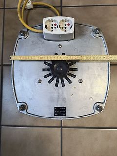
 Bild
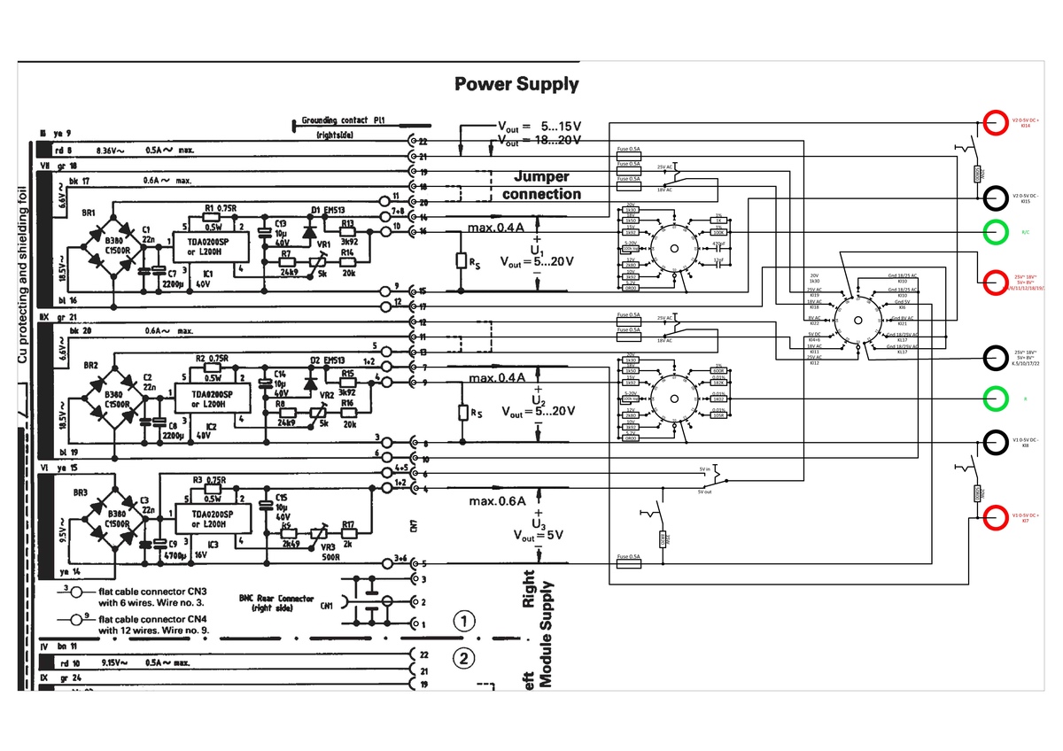
Bild
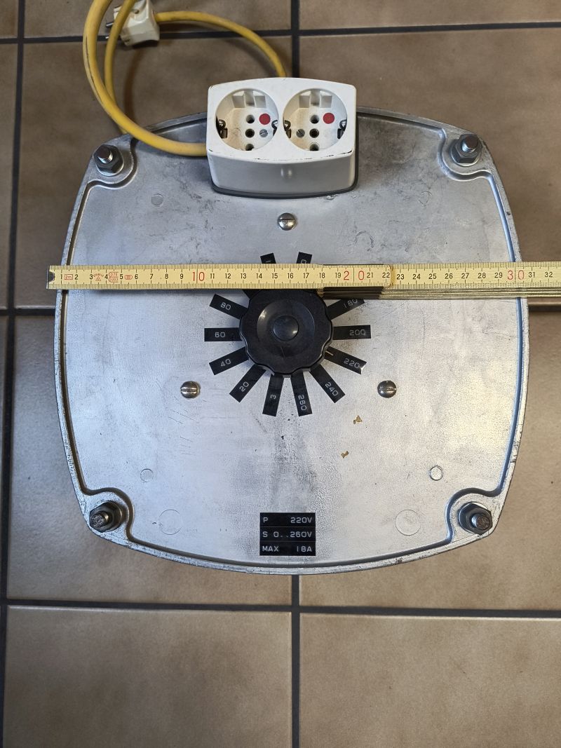
 Bild
Bild