-
PDF
SIM300_HD_V1.06.pdf
...................................50 FIGURE 27:ENTERY 1008-G60N-01R BOARD-TO-BOARD CONNECTOR PIN SIDE ..............51 FIGURE 28:ENTERY BOARD TO BOARD CONNECTOR PHYSICAL PHOTO..........................52 FIGURE 29:MOLEX 53729-0608 BOARD-TO-BOARD CONNECTOR PIN SIDE.......................52 FIGURE 30:
in „GSM sim300 mit SAM7-EX256 kommunizieren“ · Mikrocontroller und Digitale Elektronik ·
-
PDF
flyback.pdf
define vL(t) on the same side of the transformer for all subintervals. Upon making the small-ripple –V/n approximation, one obtains iC I/n – V/R v = – V L n I V C = n – R i = 0 g (4) –V/R The v (L), i (C), and i (tg waveforms are ig sketched in Fig. 3. I Application of the principle of volt- second balance to the primary-side 0 magnetizing inductance yields DT s D'Ts t Ts v = D (V ) + D' (– V ) = 0 conducting L g n (5) devices: Q 1 D1 Fig. 3. Flyback converter waveforms, continuous conduction mode. 3 Solution for the conversion
in „VIPer17L Eval“ · Analoge Elektronik und Schaltungstechnik ·
-
PDF
MSOP16.pdf
PROTRUSIONS OR GATE BURRS. MOLD FLASH, PROTRUSIONS OR GATE BURRS SHALL NOT EXCEED 0.152mm (.006") PER SIDE 4. DIMENSION DOES NOT INCLUDE INTERLEAD FLASH OR PROTRUSIONS. INTERLEAD FLASH OR PROTRUSIONS SHALL NOT EXCEED 0.152mm (.006") PER SIDE 5. LEAD COPLANARITY (BOTTOM OF LEADS AFTER FORMING) SHALL BE 0.102mm
in „IC Pinabstand für 36V zu klein ?“ · Mikrocontroller und Digitale Elektronik ·
-
Datei
btflydds_9851_rig.asm
number chararacter segments arranged like this: ;76543210 a (top bar) ;0000k--a f h j k b (f- top side bar, h- left diaginal(center to top left corner),j- vertical center,k- right diginal(cneter to top right corner), b- right top side bar) ;0000jfhb gl (g- left center, l- right center) ;0000legc e p n m c (e- left side bar,p- left diaginal (center to bottom left),n- vertical center, m- right digainal(center to bottom right corner), c- bottom right side bar ;0000mpnd d (bottom bar) gseg: ldi zl,low(2*segtable) ldi
in „ATMEGA8 + AD9833 + Nokia 3310 LCD“ · Mikrocontroller und Digitale Elektronik ·
-
PDF
EVI-370-series-instruction-manual-v1-2-eng.pdf
371D) MD-73 Board (EVI-370DG/371DG) CN101: 3P For ECCP and remote control 1. ECCP DC/UNREG OUT Board side : JST S3B-ZR-SM3A-TF 2. ECCP SIG IN/OUT Housing : JST 03ZR-8M 3. GND CN107: 4P For zoom encode 1. GND Board side : JST S4B-ZR-SM3A-TF 2. D-ZOOM POSI Housing : JST 04ZR-8M 3. ZOOM POSI 4. GND 9 EVI-370
-
PDF
MOSFET_Gate_Driver_Circuit.pdf
Toshiba Electronic Devices & Storage Corporation MOSFET Gate Drive Circuit Application Note 2.4. High-side drive from a half or full bridge Figure 2.5 shows how to use MOSFETs in a half- or full-bridge configuration. To turn on the N-channel MOSFET on the high side1Qa higher voltage against source terminal
in „MOSFET npn/pnp Driver“ · Analoge Elektronik und Schaltungstechnik ·
-
PDF
iW1816.pdf
constant current ●● Adaptively controlled soft start-up enables fast and regulation with primary-side-only feedback smooth start-up for a wide range of output voltage (5V, ●● No external compensation components required 12V and above) and capacitve loads up to 6,000μF ●● 64kHz PWM switching frequency
in „Fritz Powerline 540E abgeraucht“ · Mikrocontroller und Digitale Elektronik ·
-
PDF
MOSFET_Gate_Drive_Circuit_.pdf
Toshiba Electronic Devices & Storage Corporation MOSFET Gate Drive Circuit Application Note 2.4. High-side drive from a half or full bridge Figure 2.5 shows how to use MOSFETs in a half- or full-bridge configuration. To turn on the N-channel MOSFET on the high side1Qa higher voltage against source terminal
in „Gatebeschaltung Treiber“ · Analoge Elektronik und Schaltungstechnik ·
-
PDF
FULLTEXT01.pdf
requirements and matching the device to the output side is not always the case. For instance, loss of half the power happens on maximum power transfer and high efficiency cannot be ensured [3]. 4 2.1.3 Biasing network and stability Active device, in this
in „Buchempfehlung HF-Verstärker gesucht“ · HF, Funk und Felder ·
-
PDF
rdr-840q_30w_INN3977CQ.pdf
feedback Built-in synchronous rectification for >85% efficiency All the benefits of secondary-side control with the simplicity of primary-side regulation o Insensitive to transformer variation o Extremely fast transient response independent of load timing PATENT INFORMATION The products and applications
in „Frage zu PowerInc INN3977CQ“ · Analoge Elektronik und Schaltungstechnik ·
-
PDF
Modbus_Messaging_Implementation_Guide_V1_0b.pdf
Client to initiate a transaction, A MODBUS Indication is the Request message received on the Server side, A MODBUS Response is the Response message sent by the Server, A MODBUS Confirmation is the Response Message received on the Client side The MODBUS messaging services (Client / Server Model) are used
in „Modbus RTU Terminal, Freeware Programm“ · Mikrocontroller und Digitale Elektronik ·
-
 Bild
Bild
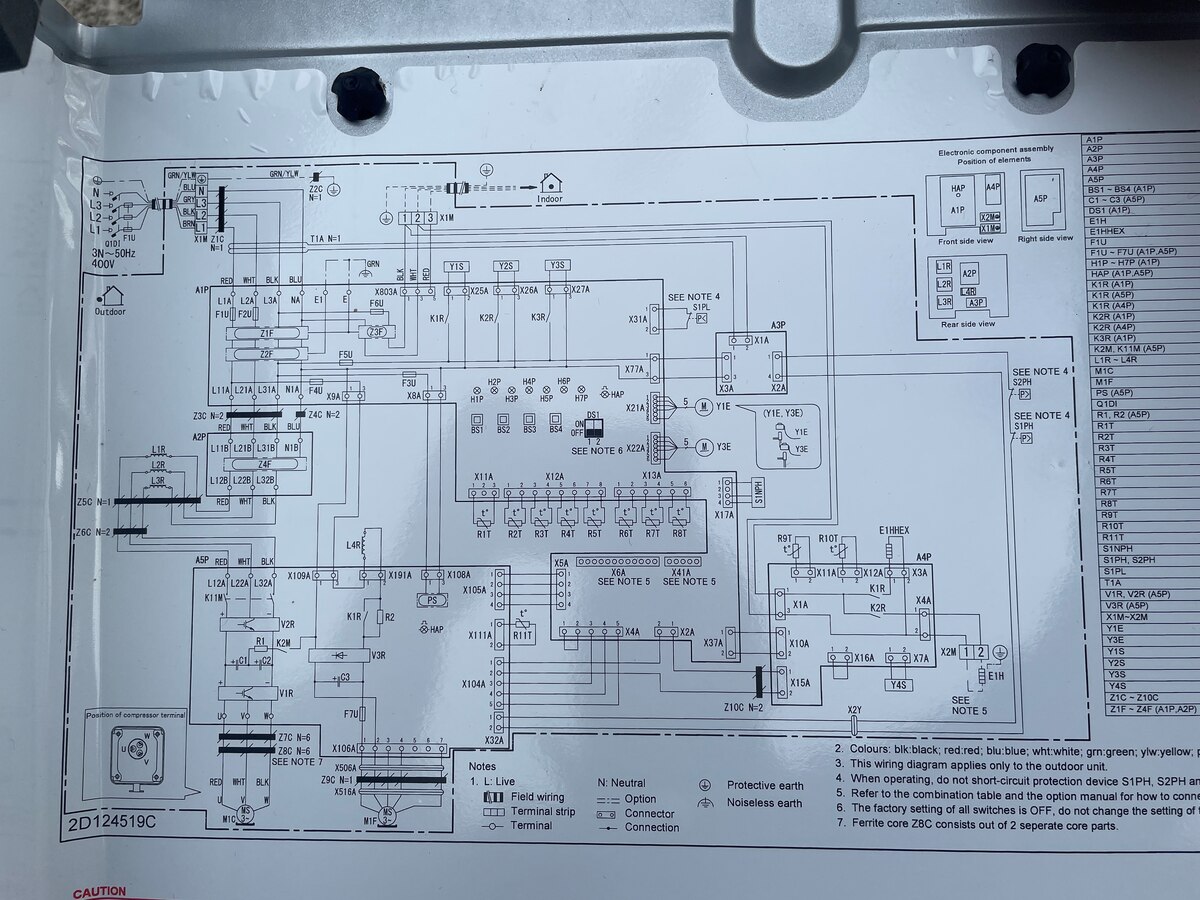
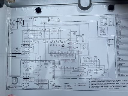
Abfotografierter Schaltplan eines elektronischen Geräts
GRN/YLW, BLK, N, L1, L2, L3, T10, 3M, 50Hz, 400V, Outdoor, A1P, A2P, A3P, A4P, HAP, ASP, Front side, Right side, Rear side, L1A, L2A, L3A, L3B, L4, L1B, L2B, L3B, L4B, Z3C, Z4C, Z5C, Z6C, Z7C, F1U, F2U, F3U, F4U, KIR, K2R, K3R, K4R, K1M, K2M, K3M, K4M, M1P, M2P, M3P, M4P, M1F, M2F, M3F, M4F, R1T,
in „PTC wird heiß, Ursache?“ · Analoge Elektronik und Schaltungstechnik · · Fotos
-
Datei
graph.py
plotRef.plot([1,2,30,4,5,6,7,8],[5,count,1,3,8,9,3,5]) canvasRef.draw() canvasRef.get_tk_widget().pack(side=tk.TOP, fill=tk.BOTH, expand=1) count=count+1 #===================== GRAPH 1 ====================================== frm1 = tk.Frame(mainWindow) frm1.place(x=200,y=60); f = Figure(figsize=(3,2), dpi=
in „Python Graphik mit tkinter und matplotlib“ · Softwareentwicklung ·
-
PDF
Eheim_Pumpe_1046_3146_universal_datenblatt.pdf
Model: see type plate on pump housing Function A Motor body fixing plate threaded adaptor, pressure side impeller-set pump cover with O-ring coarse filter suc- tion grille threaded adaptor, suction side cap. The pump can be used both in and out of the water. It is not self-priming and to operate, must
in „Ansteuerung einer 230V Pumpe mit einem 0-10V Signal“ · Analoge Elektronik und Schaltungstechnik ·
-
PDF
LT3092fb.pdf
= 0.115 0.38 ± 0.10 TYP 5 8 0.675 ±0.05 3.5 ±0.05 1.65 ±0.05 3.00 ±0.10 1.65 ± 0.10 2.15 ±0.05 (2 SIDES) (4 SIDES) (2 SIDES) PIN 1 TOP MARK PACKAGE OUTLINE (NOTE 6) (DD) DFN 1203 4 1 0.25 ± 0.05 0.25 ± 0.05 0.50 BSC 0.200 REF 0.75 ±0.05 0.50 BSC 2.38 ±0.05 2.38 ±0.10 (2 SIDES) 0.00 – 0.05 (2 SIDES) BOTTOM
in „Konstantstromquelle LT3092 - Widerstandswahl“ · Analoge Elektronik und Schaltungstechnik ·
-
PDF
MAX1758.pdf
Voltage section. 8 BATT Battery Voltage-Sense Input and Current-Sense Negative Input 9, 10 HSD High-Side Drain. This is the drain of the internal high-side FET. See Figure 3. Cell-Count Programming Input. Connect CELL to GND, REF, or VL to set 1, 3, or 4 cells, or leave uncon- 11 CELL nected to set 2 cells
in „Verständnisfrage Strom für MAX1758“ · Mikrocontroller und Digitale Elektronik ·
-
PDF
L6206.pdf
58 77 62 C/W 2 1. Mounted on a multilayer FR4 PCB with a dissipating copper surface on the bottom side of 6 cm (with a thickness of 35 µm). 2. Mounted on a multilayer FR4 PCB with a dissipating copper surface on the top side of 6 cm thickness of 35 µm). 3. Mounted on a multilayer FR4 PCB with a dissipating
in „l6206 Datenblatt Fehler?“ · Mikrocontroller und Digitale Elektronik ·
-
PDF
AS1360_Datasheet_v1_03.pdf
Descriptions Pin Number Pin Name Description Ground. This pin should be connected to the negative side of the output and the negative terminal of the input capacitor. No high-current flows out of this 1 GND pin, only bias current (1.5µA, typ). Note: Voltage drops between this pin and the negative side
in „Suche LDO mit Iss oder Iq >1uA.“ · Mikrocontroller und Digitale Elektronik ·
-
PDF
board_file_format_EN.pdf
value layer name 0 Copper layer "Copper" layers 1 to 14 Inner layers 15 Component layer 16 Copper side adhesive layer 17 Component side adhesive layer 18 Copper side Solder paste layer 19 Component Solder paste layer 20 Copper side Silk screen layer 21 Component Silk screen layer 22 Copper side Solder
-
PDF
ENG_SS_114-2025_G3.pdf
contact, including cutoff tab and burr, shall not be bent beyond the limitations given in Figure 4. Side-to-side — side-to-side bending of the contact may not exceed the limits provided in Figure 4. NOTE i Periodic inspections must be made to ensure crimped contact formation is consistent. Rev G2 5 of 11 114-2025 Up and Down Alignment 3° Max Datum Line 3° Max Side-to-Side Alignment 3° Max Datum Line 3° Max Figure 4 3.5. TensileInspection Crimped contacts should hold the wire firmly and have a pull-test tensile value meeting the values given in Figure 5. NOTE
in „Welcher Stecker ist das (Schaltbildinterpretation)“ · Fahrzeugelektronik ·
-
PDF
WIMA-Audio.pdf
the capacitor consists of two layers of film metallization and also the improved metallized on one side with aluminium. toothed attachment of the schoopage due Contacts to the leads are made through a to the enlarged spaces in the winding schoopage layer. element. have outstanding pulse behaviour. Film
in „Kondensatoren für Lautsprecherfrequenzweiche“ · Analoge Elektronik und Schaltungstechnik ·
-
PDF
bedienungsanleitung-1325476-controllino-mega-100-200-00-sps-steuerungsmodul-12-vdc-24-vdc.pdf
weiter ausgeführt. Ausgänge (D0 bis D.. und R0 bis R..) Die CONTROLLINO Steuerungen verfügt über „High-Side Switch“ und „Halb-Brücken“ (nur MEGA) Halbleiter Ausgänge und über potentialfreie Relais-Ausgänge. Die Ausgänge dienen zumSchaltenvonVerbrauchernundkönnenimUserprogrammgetrenntangesteuertwerden. Einige
in „Diode kühlen, wie?“ · Analoge Elektronik und Schaltungstechnik ·
-
PDF
Thermoelectric_Coolers_Basics.pdf
sandwiched between two ceramic plates. The latter form the hot and cold thermoelectric cooler (TEC) sides. The configuration of thermoelectric coolers is shown in Figures 2 and 3. Fig. 2 - Single-stage Thermoelectric Fig. 3 Two-stage Thermoelectric Cooler Construction Cooler Construction Commonly, a TE
in „Peltier-Kühlbox Bastelprojekt“ · Mechanik, Gehäuse, Werkzeug ·
-
 Bild
Bild
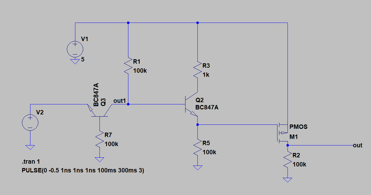
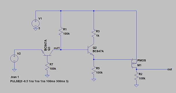
Schaltplan einer Transistorschaltung mit PMOS
V1 5 R1 100k R3 1k Q2 BC847A R5 100k M1 PMOS out R2 100k Q3 BC847A out1 V2 R7 100k .tran 1 PULSE(0 -0.5 1ns 1ns 100ms 300ms)
in „High Side Switch Mosfet“ · Analoge Elektronik und Schaltungstechnik · · Schaltpläne
-
PDF
ADC_Side_with_identified_Analog_Input_Pins.pdf
ADC_Side_with_identified_Analog_Input_Pins.pdf
in „Wittig(welec) DSO W20xxA Hardware (Teil 2)“ · Mikrocontroller und Digitale Elektronik ·
-
PDF
SuperSID_V3-R3_Schematic.PDF
SuperSID_V3-R3_Schematic.PDF
in „Operationsverstärker gesucht“ · Analoge Elektronik und Schaltungstechnik ·
-
 Bild
Bild
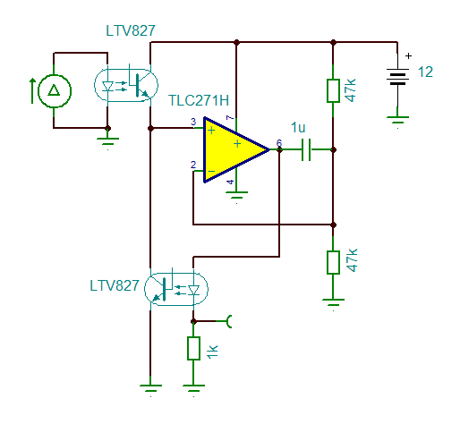
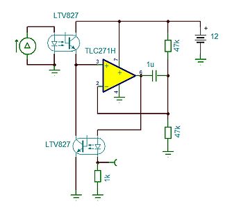
Schaltplan mit Operationsverstärker und Optokopplern
LTV827 TLC271H 1u 47k 12 47k 1k
in „Lineare High-Side-Strommessung mit Optokopplern“ · Analoge Elektronik und Schaltungstechnik · · Schaltpläne
-
PDF
MPQ4210_r1.1_MPS.pdf
) ILG_SO CC 0.85 A HG_SI 1.6 A Gate sink current capability) VCC = 7.2V, 4.7nF load LG_SI 2 A Low-side gate output high V CC- voltage V LS_HIGH 0.05 V Low-side gate output low V LS_LOW 0.05 V voltage High-side gate output high VBST-SW voltage V HS_HIGH 0.05 V High-side gate output low V HS_LOW 0.05 V voltage Dead-time between high-side gate and low-side gate(8) T DEAD 30 ns OVP Protection FB feedback OVP trigger V 119% 127% 135% V threshold OVP_RISING REF FB feedback OVP recover VOVP_FALLING 104% 111% 118% VREF threshold Thermal Protection
in „Controlling DC DC converter with STM32“ · Analoge Elektronik und Schaltungstechnik ·
-
PDF
ruin_sorbees.pdf
be fine." Room Service: "We bother?" "With butter?" Hotel Guest: "No, just put the bother on the side." Room Service: "Wad?" "What?" Hotel Guest: "I mean butter...just put it on the side." Room Service: "Copy?" "Coffee?" Hotel Guest: "Sorry?" Room Service: "Copy...tea...mill?" "Coffee...tea...milk?"
in „Tutorials und Lehrvideos in englische Sprache von Indern vorgetragen.“ · Offtopic ·
-
PDF
Ablerex_ESx000_AS3100_09TH0459_2.pdf
_2 Bottom Side (PVBD020) Page 129 of 167 Report No. 09TH0459-AS3100_2 ES2200 / ES3300 / ES4400 / ES5000 EMI Board (PVBF000) Page 130 of 167 Report No. 09TH0459-AS3100_2 Top Side (PVBF000) Bottom Side (PVBF000) Page
in „Wechselrichter effekta es 5000 streikt“ · Analoge Elektronik und Schaltungstechnik ·
-
 Bild
Bild
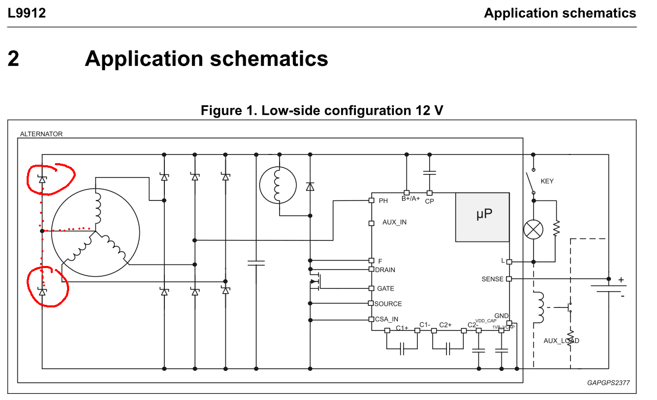
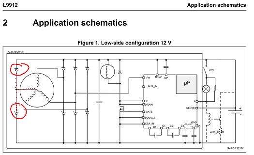
Schaltplan einer Low-side Konfiguration 12 V für einen Alternator
L9912 Application schematics 2 Figure 1. Low-side configuration 12 V ALTERNATOR KEY μP L SENSE GND AUX_LOAD + AUX_IN F DRAIN GATE SOURCE CSA_IN C1+ C1- C2+ C2- VDD_CAP GND 1V8
in „Identifikation von Dioden erbeten“ · Fahrzeugelektronik · · Schaltpläne
-
PDF
sloa069.pdf
is placed near the power pin, there is a long connection to the ground pin, and access to the left side of the IC is restricted on one layer. • If the capacitor is placed near the ground pin, there is a long connection to the power pin, and access to the right side of the IC is restricted on one layer. • If the connections are made underneath the IC, there is free access to both sides of the IC on all layers, but access beneath the IC is blocked, and nothing is done to alleviate long connections. • The capacitor can be placed on the bottom side of the PCB (not shown), which will
in „zwei kl. Verständnisfragen“ · Mikrocontroller und Digitale Elektronik ·
-
PDF
SLOA069__How__Not__To_Decouple_High-Speed_Operational_Amplifiers.pdf
is placed near the power pin, there is a long connection to the ground pin, and access to the left side of the IC is restricted on one layer. • If the capacitor is placed near the ground pin, there is a long connection to the power pin, and access to the right side of the IC is restricted on one layer. • If the connections are made underneath the IC, there is free access to both sides of the IC on all layers, but access beneath the IC is blocked, and nothing is done to alleviate long connections. • The capacitor can be placed on the bottom side of the PCB (not shown), which will
in „Berechnungsprogramme Coplanare Mikrostripleitungen mit Ground“ · HF, Funk und Felder ·
-
PDF
How__Not__To_Decouple_High-Speed_Operational_Amplifiers.pdf
is placed near the power pin, there is a long connection to the ground pin, and access to the left side of the IC is restricted on one layer. • If the capacitor is placed near the ground pin, there is a long connection to the power pin, and access to the right side of the IC is restricted on one layer. • If the connections are made underneath the IC, there is free access to both sides of the IC on all layers, but access beneath the IC is blocked, and nothing is done to alleviate long connections. • The capacitor can be placed on the bottom side of the PCB (not shown), which will
in „Welchen 100nF Entkoppelungskondensator für bis zu 7GHz“ · HF, Funk und Felder ·
-
PDF
WhatsAllThisBoxStuffAnyhow.pdf
and also over one or more of our precision calibrated platinum thermometers. We set up two sockets side-by-side so we could put in two units and cross-compare them with quicker response, because devices in the same package will have about the same time-constant. After a few days, one of the technicians
in „Raumtemperatur messen mit LM75“ · Analoge Elektronik und Schaltungstechnik ·
-
PDF
Platte_neu_2.pdf
5 RA3/AN3/VREF+ RB3/AN9/CCP2/VPO 36 -15V 6 RA4/T0CKI/CIOUT/RCV RB2/AN8/INT2/VMO 35 PWM OP_1_HIGH_SIDE_LEFT 7 RA5/AN4/SS/HLVDIN/C2OUT RB1/AN10/INT1/SCK/SCL34 RPM +15V_T1 +15V_T1 8 RE0/AN5/CK1SPP RB0/AN12/INT0/LFT0/SDI/SDA3 BRAKE_SIGNAL 8 9 RE1/AN6/CK2SPP VDD 32 +5V 10 31 2 7 C18 +C17 11 RE2/AN7/OESPP
in „Schaltung H-Brücke mit µC und Zubehör“ · Mikrocontroller und Digitale Elektronik ·
-
PDF
6neds.pdf
EID1 EID 0 016416/036416 SID10 SID9 SID 8 SID7 SID 6 SID 5 SID4 SID3 SID2 SID1 SID 0 016616/036616 CANi local 016816/036816 EID 17EID16EID 15EID14 EID13EID 12EID11EID 10 EID9 EID8 EID7 EID 6 mask A register EID 5 EID4 EID3 EID
in „M16C- Key Input Interrupt“ · Mikrocontroller und Digitale Elektronik ·
-
PDF
lcd1.pdf
located on the any of the display types. place to the left. The cursor will re-appear right-hand side of the display. As numbers The relationship between addresses and from the right-hand side, immediately after are entered, they move to the left, leaving display locations varies, depending on the the
in „eigene Zeichen im LCD darstellen“ · Mikrocontroller und Digitale Elektronik ·
-
PDF
MAX1920-MAX1921.pdf
T = +25°C, unless otherwAse noted.) (Note 1) PARAMETER SYMBOL CONDITIONS MIN TYP MAX UNITS X Low-Side Current Limit ILIMN 350 550 800 mA 1 9 High-Side On-Resistance R ONHS ILX = -40mA, V = 3IN 0.6 1.1 Ω 2 Rectifier On-Resistance R ONSR ILX = 40mA, V IN = 3V 0.5 0.9 Ω 0 Rectifier Off-Current Threshold
in „Sinnvoll, von 3V Solar mit Stepdown auf 2,5V SuperCap ?“ · Mikrocontroller und Digitale Elektronik ·
-
PDF
73d.pdf
the laser diode. As it is well known, we can take the optical output of the interferometer from two sides (Fig. 1): i) from a photodetector PD2 placed behind the laser chip, opposite to the target side, usually the monitor photodiode provided by the manufacturer for monitoring the emitted power (this is
in „Effekte in Laserdiode bei reflektiertem Strahl“ · Analoge Elektronik und Schaltungstechnik ·
-
PDF
how_to_use_cdm_1.pdf
located on the any of the display types. place to the left. The cursor will re-appear right-hand side of the display. As numbers The relationship between addresses and from the right-hand side, immediately after are entered, they move to the left, leaving display locations varies, depending on the the
in „Dokumentation gesucht (UC121902-TNARX-A)“ · Mikrocontroller und Digitale Elektronik ·
-
PDF
Maestro_GPS_Receiver_A2035_H_User_Manual_V1_3.pdf
.........................................................................17 4.1 Details Component Side A2035-H ..................................................................17 4.2 Details Solder Side A2035-H ..........................................................................18 5 Pin-out Information
in „Schlampiges GPS-Receiver Datenblatt (Maestro 2035-H)“ · Mikrocontroller und Digitale Elektronik ·
-
PDF
WAGO_Kontakttechnik_GmbH___...pdf
WAGO KontakttechnikGmbH & Co. KG http://www.wago.com/cps/rde/xchg/SID-53EFFEF9-D10A74EC/wago/... WAGO Kontakttechnik GmbH & Co. KG, Hansastrasse 27, D-32423 Minden, Tel ++49/571/887-0, e-mail: info@wago.com 1 von3 15.04.2009 16:08 WAGO KontakttechnikGmbH & Co. KG http://www.wago.com/cps/rde/xchg/SID-53EFFEF9-D10A74EC/wago/... Linux bietet für die Automatisierung mehr Zuverlässigkeit und Investitionssicherheit als viele kommerzielle Betriebssysteme. Deswegen setzt WAGO bei seinen Linux-Controllern
in „Steuergerät / Schaltmodul, TCP/IP, Automation“ · Haus & Smart Home ·
-
PDF
SV1-505A.pdf
France E130092 Compound Isostac D45003 SAS TESTING DETAILS: MECHANICAL SPECIFICATION: Front View: Side View: Test condition @ 50Hz: Input voltage (N1) = 10V (9.9 to 10.1)V 21.5 Max 19 Max No load current = 8mA to 9mA Maximum Output voltage Uo = 1.0V (0.88 to 1.02)V SV1-505A x . Inductance: 1 : 10 M 1
in „LTSpice: Sprung im Strom durch Diode“ · Analoge Elektronik und Schaltungstechnik ·
-
PDF
TSL237-E21.pdf
Options DEVICE TA PACKAGE − LEADS PACKAGE DESIGNATOR ORDERING NUMBER TSL237 −25⋅C to 70⋅ Single In-Line Side-Looker S TSL237S The LUMENOLOGY ▯ Company ▯ Copyright ▯ 2004, TAOS Inc. Texas Advanced Optoelectronic Solutions Inc. 800 Jupiter Road, Suite 205 ▯ Plano, TX 75074 ▯ (972) 673-0759 www.taosinc.com 1
in „Frequenzzähler + digitales Filter mit pic10“ · Digitale Signalverarbeitung / DSP / Machine Learning ·
-
PDF
EGS002_manual_en.pdf
Ground 3 1LO O Right bridge low sidegate drive output 4 GND GND Ground 5 VS1 O Right bridge high side floating supply return 6 1HO O Right bridge high side gate drive output 7 GND GND Ground 8 2LO O Left bridge low side gate drive output 9 VS2 O Left bridge high side floating supply return 10 2HO O Left bridge high side gate drive output Copyright 2014©EGmicro corp. www.EGmicro.com 2 / 6 micro corp. EGS002 Datasheets EG8010 demo board 11 GND GND Ground 12 +12V +12V +12V voltage input. (range: 10V-15V) 13 GND GND Ground
in „EGS002 welches Display ist geeignet ?“ · Mikrocontroller und Digitale Elektronik ·
-
PDF
EGS002_manual.pdf
Ground 3 1LO O Right bridge low sidegate drive output 4 GND GND Ground 5 VS1 O Right bridge high side floating supply return 6 1HO O Right bridge high side gate drive output 7 GND GND Ground 8 2LO O Left bridge low side gate drive output 9 VS2 O Left bridge high side floating supply return 10 2HO O Left bridge high side gate drive output Copyright 2014©EGmicro corp. www.EGmicro.com 2 / 6 micro corp. EGS002 Datasheets EG8010 demo board 11 GND GND Ground 12 +12V +12V +12V voltage input. (range: 10V-15V) 13 GND GND Ground
in „Inverter DC/AC mit EGS002 China DEV-Board“ · Analoge Elektronik und Schaltungstechnik ·
-
PDF
22100128_MA_01.pdf
T ist schaltbar auf 0 - 125 Volt und 125 - 250 Volt. In of the voltage switch located at the left side. The fuse of R diesen Bereichen läßt sich die Ausgangsspannung an this output is M 4A(for 3A-Version)other M6,3A(for 4,5A- der Ausgangssteckdose einstellen. Der Ausgang ist mit Version) and located
in „Netzteil nach einem Kurzschluss am Ausgang defekt“ · Analoge Elektronik und Schaltungstechnik ·
-
PDF
22100128_MA_01.pdf
T ist schaltbar auf 0 - 125 Volt und 125 - 250 Volt. In of the voltage switch located at the left side. The fuse of R diesen Bereichen läßt sich die Ausgangsspannung an this output is M 4A(for 3A-Version)other M6,3A(for 4,5A- der Ausgangssteckdose einstellen. Der Ausgang ist mit Version) and located
in „Was ist ein Entlötwiderstand (10Ω, 10W) ?“ · Analoge Elektronik und Schaltungstechnik ·
-
PDF
LDD-nnnL.pdf
1 3 4 4 1 (Red) PWM DIM ON/OFF andPWM Dimming 3 (White) (Leave openif not used) BOTTOM SIDE -Vin VIEW VIEW 4 (Black) Don't connect to -Vout 5 -Vout LED - Connection 5±2mm 100±10mm (Blue) 6 5 +Vout 5 6 LED + Connection (Yellow) NOTE: Allwires UL3385 22AWG S type(LDD - 300~700LS): 17.78 [0.70
in „LDD-300 und BAM“ · Mikrocontroller und Digitale Elektronik ·