-
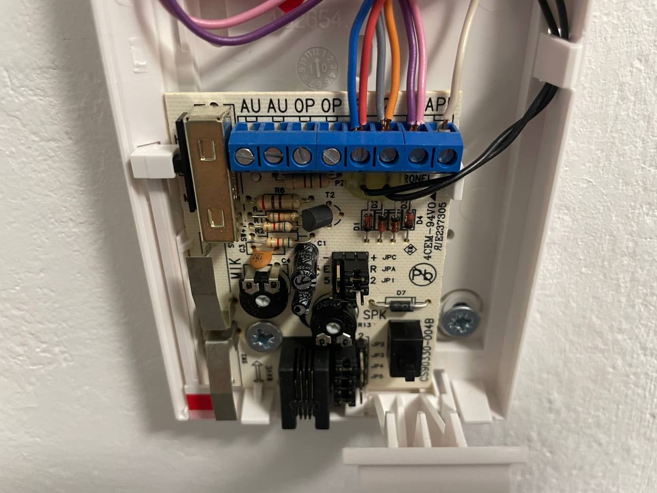
 Bild
Innenansicht einer Platine mit Anschlussklemmen und Bauteilen
AU AU OP OP AP RONEL C1 C2 C4 C5 C6 C7 C8 C9 C10 C11 C12 C13 C14 C15 C16 C17 C18 C19 C20 C21 C22 C23 C24 C25 C26 C27 C28 C29 C30 C31 C32 C33 C34 C35 C36 C37 C38 C39 C40 C41 C42 C43 C44 C45 C46 C47 C48 C49 C50
in „ESP32/Arduino: Türklingelsignal detektieren und schalten“ · Analoge Elektronik und Schaltungstechnik · · Platinenfotos
-
Datei
MCP6561.txt
******************************************************************************** * * The following op-amps are covered by this model: * MCP6561/1R/1U/2/4 * * Date of model creation: 4/9/2011 * * Revision History: * REV A: 31-Jan-11, Created model * REV B: 09-Apr-11, Fixed output voltage swing * * Recommendations
in „Konstantsromquelle für 3W LED“ · Analoge Elektronik und Schaltungstechnik ·
-
Datei
MCP6566.txt
******************************************************************************** * * The following op-amps are covered by this model: * MCP6566/6R/6U/7/9 * * * Revision History: * REV A: 14-Mar-11, Created model * REV B: 09-Apr-11, Fixed output voltage swing * * Recommendations: * Use PSPICE (or SPICE
in „PSpice Modell in LTSpice Problem“ · Mikrocontroller und Digitale Elektronik ·
-
PDF
tl072.pdf
13.97 11230 4.32 TL074ACNE4 N PDIP 14 25 506 13.97 11230 4.32 TL074BCD D SOIC 14 50 507 8 3940 4.32 TL074BCDE4 D SOIC 14 50 507 8 3940 4.32 TL074BCN N PDIP 14 25 506 13.97 11230 4.32 TL074BCNE4 N PDIP 14 25 506 13.97 11230 4.32 TL074CD D SOIC 14 50 507 8 3940 4.32 TL074CDG4 D SOIC 14 50 507 8 3940 4.32 TL074CN N PDIP 14 25 506 13.97 11230 4.32 TL074CN N PDIP 14 25 506 13.97 11230 4.32 TL074CNE4 N PDIP 14 25 506 13.97
in „Verstärkerschaltung läuft nicht wie gewollt“ · Analoge Elektronik und Schaltungstechnik ·
-
PDF
catalog.pdf
: Amplifiers - Op Amps, Buffer, Instrumentation [Desc]: Op Amp Single Precision Amplifier R-R O/P ±15V 8-Pin SOIC N Tube MPN: OPA121KU/2K5E4 [ID]: 000082 [Price]: undef/offer [QTY]: 5 [Category]: Amplifiers - Op Amps,
-
Datei
rfm12.inc
Receiver Control Command ldi YH, 0x94 ; VDI, Fast response, 67kHz ldi YL, 0xa0 ; LNA: -14db, RSSI: -97dBm rcall rfm_com_send ; Data Filter ldi YH, 0xc2 ; Enable Clock recover, Disable recover fast mode, Digital Filter (s=0) ldi YL, 0xac ; DQD Treshold sollte <4 sein wenn Bitrate zu nah an Regelabweichung
in „RFM12 Statusabfrage“ · Mikrocontroller und Digitale Elektronik ·
-
PDF
OP07.pdf
in two standard performance grades. The The OP07 has very low input offset voltage (75 μV maximum for OP07E is specified for operation over the 0°C to 70°C range, OP07E) that is obtained by trimming at the wafer stage. These and the OP07C is specified
in „Spannungsregler für Operationsverstärker“ · Analoge Elektronik und Schaltungstechnik ·
-
PDF
OP07_a.pdf
also features low input bias current (±4 nA for OP07E is specified for operation over the 0°C to 70°C range, and OP07E) and high open-loop gain (200 V/mV for OP07E). The OP07C over the –40°C to +85°C temperature range. low offsets and high open-loop
in „Anfängerfrage Ltspice, Operationsverstärker“ · Analoge Elektronik und Schaltungstechnik ·
-
PDF
penhub.pdf
100n 100n 100n 100n 100n 100n 47 VSS MISO1 PB4 56 MISO 2 1 2 8 31 VSS 18 VSS +3.3V LiMnO2, 74AUP1G97 74AUP1G97 MC74HC4060A kein Akku? BATT-ON_H BATT-ON_H 4 k R 1 +3.3V BATT-TEST_H BATT-TEST_H CSB_H V11 PB1 27 BC846 3 B Q3 7 13 B Q3 9 PB2 28 CSA_H 2 A Q2 6 14 A Q2 10 BATT_V 25 PC5 ADC.14 CMP1P WKUP5
in „Datenlogger Pendeluhr“ · Mikrocontroller und Digitale Elektronik ·
-
PDF
AN101_An_Introduction_to_FETs_70594__VIS.pdf
field-effect transistor was known as a “unipolar” transis- FET groups depend on different phenomena for their op- tor. The term refers to the fact that current is transported eration, and will be discussed separately. by carriers of one polarity (majority), whereas in the con- ventional bipolar transistor carriers
in „mit 2,7V schalten“ · Mikrocontroller und Digitale Elektronik ·
-
PDF
ICE2AS01.pdf
0.3V PWM-Latch 0.3V Gate Driver t Oscillator C5 V Gate Driver OSC 0.8V 10kΩ x3.65 t T2 R 1 V 1 PWM OP Figure 7 Light Load Conditions C 1 20pF 3.2.1 PWM-OP Voltage Ramp The input of the PWM-OP is applied over the internal leading edge blanking to the external sense resistor Figure 6 Improved Current Mode
in „TFT LP mit IC ICE2AS01 defekt“ · Mikrocontroller und Digitale Elektronik ·
-
PDF
OP07.pdf
features low input bias current (±4 nA for the OP07Eisspecifiedforoperationoverthe0°Cto70°Crange, and OP07E) and high open-loop gain (200 V/mV for the OP07E). theOP07Cisspecifiedover the–40°Cto+85°Ctemperaturerange. The low offsets and high open-loop
in „Gleichrichteschaltung mittels op“ · Analoge Elektronik und Schaltungstechnik ·
-
PDF
P82B96_7.pdf
Product data sheet - P82B96_6 Modifications: • Table 1 ÒOrdeirng informatio: changed type number from ÒP82B96TD/S410Ó to ÒP82B96TD/S900Ó • Table 2 ÒOrdeirng option: changed type number from ÒP82B96TD/S410Ó to ÒP82B96TD/S900Ó • Figure 3 ÒPin conguration for SO8: changed type number from ÒP82B96TD/S410Ó to ÒP82B96TD/S900Ó • Table 4 ÒLimitingaluesÓ, Conditions column for symbol T: changed from ÒP82B96TD/S410Ó j to ÒP82B96TD/S900Ó • Table 5 ÒChaarcteristic, Table note [1]: changed from ÒP82B96TD/S410Ó to ÒP82B96TD
in „18 x SHT11 an welchem Mikrocontroller“ · Mikrocontroller und Digitale Elektronik ·
-
PDF
6502_Schematic.pdf
Cp2 Cp2 A7 x8 DATA1 x1 Cp1 x2 x2 x3 x4 x5 x6 x7 Cp2 Carry7,out ADDR1 Cp2 Carry ADDR2 x3 Cp2 x5 x7 1. op. Cp2 DATA2 x4 ADDR2 DATA1 x1 x0 Carry 2. op. x3 DATA1 x1 ADDR2 x1 x5 D6 x1 x3 Carry x3 x2 SUM EOR NOR x2 x2 x4 DATA1 x12 x9 x3 Cp2 Cp2 ADDR1 x6 x3 ADDR1 x2 x4 XOR7 x15 ADDR1 Cp2 x4 x20,6 ALU6 x14 DATA2
in „Frage zu Sprungvorhersagen bei modernen CPUs“ · PC Hard- und Software ·
-
PDF
6502_Schematic.pdf
Cp2 Cp2 A7 x8 DATA1 x1 Cp1 x2 x2 x3 x4 x5 x6 x7 Cp2 Carry7,out ADDR1 Cp2 Carry ADDR2 x3 Cp2 x5 x7 1. op. Cp2 DATA2 x4 ADDR2 DATA1 x1 x0 Carry 2. op. x3 DATA1 x1 ADDR2 x1 x5 D6 x1 x3 Carry x3 x2 SUM EOR NOR x2 x2 x4 DATA1 x12 x9 x3 Cp2 Cp2 ADDR1 x6 x3 ADDR1 x2 x4 XOR7 x15 ADDR1 Cp2 x4 x20,6 ALU6 x14 DATA2
in „LED Lauf-/Blinklicht in DIY Spielzeug“ · Analoge Elektronik und Schaltungstechnik ·
-
PDF
lt8645s-8646s.pdf
> 0.97V, V = 0V, V = 5V 16 25 µA EN/UV FB SYNC BIAS LT8646S BIAS Quiescent Current in Sleep VEN/UV = 2V, FB> 0.97V, VSYNC= 0V, VBIAS= 5V 200 260 µA LT8645S V INQuiescent Current when Active VEN/UV = 2V, FB> 0.97V, VSYNC= 2V, RT= 60.4k, VBIAS= 0V 0.4 0.6 mA LT8646S V INQuiescent Current when Active VEN/UV = 2V, FB> 0.97V, VSYNC= 2V, RT= 60.4k, VBIAS= 0V 0.6 0.8 mA LT8645S V INCurrent in Regulation VOUT = 0.97V
in „LT8645 / LT8646 brennt durch.“ · Analoge Elektronik und Schaltungstechnik ·
-
PDF
TB12To5.pdf
es {Rx}. Dann muß noch das Step-Kommando eingefügt werden. Dazu in der Menüleiste oben rechts auf „.op“ klicken. Im sich öffnenden Fenster die Direktive: .step param Rx 25 250 225 schreiben. Das bedeutet, der Widerstandswert „Rx“ von Rload beginnt mit 25 Ohm und endet bei 250 Ohm, die Schrittweite ist
in „Diskreter DC/DC-Wandler in LtSpice“ · Analoge Elektronik und Schaltungstechnik ·
-
PDF
Medugu_et_al.pdf
negligibly small, over the photosynthetically active wavelengths. Medugu et al. 1721 C r 220pF R f0K +9V Op. Amp + V C c R c 220pF 1K - Figure 2. Pyranometer circuit diagram. The choice of pyranometer detector (photodiode) has seen later. Finally, Rf is the feedback resistor which fixes required an exhaustive
in „Sonnenscheindauer Sensor selber bauen Eigenbau ATmega Assembler“ · Projekte & Code ·
-
PDF
PCD8544_1.pdf
system 0 0 0 0 1 0 BS BS BS set Bias System (BS ) 2 1 0 x Reserved 0 0 1 X X X X X X do not use Set OP 0 1 VOP6 VOP5 VOP4 VOP3 VOP2 VOP1 VOP0 writeOP to register Table 2 Explanations of symbols in Table 1 BIT 0 1 PD chip is active chip is in Power-down mode V horizontal addressing vertical addressing
in „(Dieser Beitrag wurde geloescht)“ · Mikrocontroller und Digitale Elektronik ·
-
PDF
pcd8544.pdf
system 0 0 0 0 1 0 BS BS BS set Bias System (BS ) 2 1 0 x Reserved 0 0 1 X X X X X X do not use Set OP 0 1 VOP6 VOP5 VOP4 VOP3 VOP2 VOP1 VOP0 writeOP to register Table 2 Explanations of symbols in Table 1 BIT 0 1 PD chip is active chip is in Power-down mode V horizontal addressing vertical addressing
-
PDF
PCD8544_1.pdf
system 0 0 0 0 1 0 BS BS BS set Bias System (BS ) 2 1 0 x Reserved 0 0 1 X X X X X X do not use Set OP 0 1 VOP6 VOP5 VOP4 VOP3 VOP2 VOP1 VOP0 writeOP to register Table 2 Explanations of symbols in Table 1 BIT 0 1 PD chip is active chip is in Power-down mode V horizontal addressing vertical addressing
in „MSP430F2013 steuert Nokia-3310-Display an“ · Mikrocontroller und Digitale Elektronik ·
-
PDF
PCD8544_-_3310_Display_Controler.pdf
system 0 0 0 0 1 0 BS BS BS set Bias System (BS ) 2 1 0 x Reserved 0 0 1 X X X X X X do not use Set OP 0 1 VOP6 VOP5 VOP4 VOP3 VOP2 VOP1 VOP0 writeOP to register Table 2 Explanations of symbols in Table 1 BIT 0 1 PD chip is active chip is in Power-down mode V horizontal addressing vertical addressing
in „Atmega8 Nokia 3310 Display und AVR-Studio“ · Mikrocontroller und Digitale Elektronik ·
-
PDF
Nokia5510LCD_datasheet.pdf
system 0 0 0 0 1 0 BS BS BS set Bias System (BS ) 2 1 0 x Reserved 0 0 1 X X X X X X do not use Set OP 0 1 VOP6 VOP5 VOP4 VOP3 VOP2 VOP1 VOP0 writeOP to register Table 2 Explanations of symbols in Table 1 BIT 0 1 PD chip is active chip is in Power-down mode V horizontal addressing vertical addressing
in „Probleme mit Taktversorgung auf Steckbrett“ · Mikrocontroller und Digitale Elektronik ·
-
PDF
Nokia5510LCD_datasheet.pdf
system 0 0 0 0 1 0 BS BS BS set Bias System (BS ) 2 1 0 x Reserved 0 0 1 X X X X X X do not use Set OP 0 1 VOP6 VOP5 VOP4 VOP3 VOP2 VOP1 VOP0 writeOP to register Table 2 Explanations of symbols in Table 1 BIT 0 1 PD chip is active chip is in Power-down mode V horizontal addressing vertical addressing
in „[PIC]Probleme bei SPI Übertragung“ · Mikrocontroller und Digitale Elektronik ·
-
PDF
PCD8544_-_3310_Display_Controler.pdf
system 0 0 0 0 1 0 BS BS BS set Bias System (BS ) 2 1 0 x Reserved 0 0 1 X X X X X X do not use Set OP 0 1 VOP6 VOP5 VOP4 VOP3 VOP2 VOP1 VOP0 writeOP to register Table 2 Explanations of symbols in Table 1 BIT 0 1 PD chip is active chip is in Power-down mode V horizontal addressing vertical addressing
in „Display Nokia 5110“ · Mikrocontroller und Digitale Elektronik ·
-
PDF
Nokia5110.pdf
system 0 0 0 0 1 0 BS BS BS set Bias System (BS ) 2 1 0 x Reserved 0 0 1 X X X X X X do not use Set OP 0 1 VOP6 VOP5 VOP4 VOP3 VOP2 VOP1 VOP0 writeOP to register Table 2 Explanations of symbols in Table 1 BIT 0 1 PD chip is active chip is in Power-down mode V horizontal addressing vertical addressing
in „Nokia 5110 ansteuern für newbie“ · Mikrocontroller und Digitale Elektronik ·
-
PDF
Gesamtinhalt_1987-2016.pdf
1995/2 67 - 85 Erkenntnisse DJ 7 FJ Ein logarithmischer ZF-Verstärker Dr. -Ing. J. Jirmann, 1995/2 97 - 101 hoher Genauigkeit DB 1 NV Achtung, Parasiten! D. Eckart Schmitzer, 1995/3 140 - 144 DJ 4 BG Design und Realisierung von Mikro- Gunthard Kraus, 1995/2 120 - 125 wellenschaltungen,Teil 1 DG 8 GB
-
PDF
catalog.pdf
: Amplifiers - Op Amps, Buffer, Instrumentation [Desc]: Op Amp Single Precision Amplifier R-R O/P ±15V 8-Pin SOIC N Tube MPN: OPA121KU/2K5E4 [ID]: 000082 [Price]: undef/offer [QTY]: 5 [Category]: Amplifiers - Op Amps,
-
PDF
CD40110B.pdf
Orderable Status Material type Package | Pins Package qty | Carrier RoHS Lead finish/ MSL rating/ Op temp (°C) Part marking part number (1) (2) (3) Ball material Peak reflow (6) (4) (5) CD40110BE Active Production PDIP (N) | 16 25 | TUBE Yes NIPDAU N/A for Pkg Type -55 to 125 CD40110BE (1)Status: For
in „Timer 555 Experimentierplatine“ · Analoge Elektronik und Schaltungstechnik ·
-
PDF
eusi98lm.pdf
for the corresp onding Hilb erttransformer whose rejec- q 4 1 tion band isde▯ned over 0:53 < f < 0:97. This way, the 1 ▯ 1 ▯ 2 1 L design ofthe halfband ▯lterand the Hilbert transformer t = q (16) 2 4 1 1 + 1 ▯ are regarded as a phase approximation problem. Since 2 L the Hilb erttransformer isusually
in „Hilbert Transformation im uC berechnen“ · Digitale Signalverarbeitung / DSP / Machine Learning ·
-
PDF
TB12To5.pdf
es {Rx}. Dann muß noch das Step-Kommando eingefügt werden. Dazu in der Menüleiste oben rechts auf „.op“ klicken. Im sich öffnenden Fenster die Direktive: .step param Rx 25 250 225 schreiben. Das bedeutet, der Widerstandswert „Rx“ von Rload beginnt mit 25 Ohm und endet bei 250 Ohm, die Schrittweite ist
in „Diskreter DC/DC-Wandler in LtSpice“ · Analoge Elektronik und Schaltungstechnik ·
-
Datei
main.lss.txt
(prog_state 972: 80 91 62 00 lds r24, 0x0062 976: 81 30 cpi r24, 0x01 ; 1 978: 09 f4 brne .+2 ; 0x97c <usbFunctionWrite+0x24> 97a: b7 c0 rjmp .+366 ; 0xaea <usbFunctionWrite+0x192> 97c: 84 30 cpi r24, 0x04 ; 4 97e: 09 f4 brne .+2 ; 0x982 <usbFunctionWrite+0x2a> 980: b4 c0 rjmp .+360 ; 0xaea <usbFunctionWrite
in „2 Programme in einem AVR“ · Mikrocontroller und Digitale Elektronik ·
-
PDF
AD5933.pdf
.............................................................................14 Register Address 0x97).............................................................. 27 Frequency Sweep Command Sequence...................................15 Serial Bus Interface...........................................
in „Spannungsmessung bei der Impedanzspektroskopie“ · Mikrocontroller und Digitale Elektronik ·
-
Datei
8080int-jmp.asm
,ZFL_C ; | rjmp op_da_a02 ; if (C flag ... cpi opl,0x90 ; |... or upper nibble >= 0x90) brlo op_da_a03 ; | op_da_a02: ori oph,0x60 ; add 0x60 ori temp2,(1<<ZFL_C) ; set new C flag op_da_a03: ; endif rjmp op_da_ae op_da_a10
in „CP/M auf ATmega88“ · Mikrocontroller und Digitale Elektronik ·
-
Datei
8080int-jmp.asm
,(1<<ZFL_C) rjmp op_da_60 cpi opl,0xa0 brlo op_da_60n op_da_60: ori oph,0x60 op_da_60n: cpi opl,0x9a brlo op_da_99n ori z_flags,(1<<ZFL_C); set C op_da_99n: sbrs z_flags,ZFL_N ; if sub-op rjmp op_da_add ; then sub opl,oph
in „CP/M auf ATmega88“ · Mikrocontroller und Digitale Elektronik ·
-
PDF
Z80-Zilog.pdf
Bits Affected None. Example If Index Register IY contains the numbA940h , the instruction LD (IY+10h97h results in byt97h in memory locationA950h . UM008011-0816 Z80 Instruction Description Z80 CPU User Manual 88 LD A, (BC) Operation A ← (BC) Op Code LD Operands A, (BC) 0 0 0 0 1 0 1 0 0A Description
in „DDR Schach-Computer Chess Master Diamond reparieren (Dauerton)“ · Mikrocontroller und Digitale Elektronik ·
-
PDF
Schematic_Prints__1_.pdf
R910 5 R911 100k ADCIN5 B ADC1 OP_OUT17 ADC5 OP_OUT57 B ADC1 6 ADC5 6 R914 4.02k R915 4.02k C902 LMV324IDR R912 C903 LMV324IDR R913 1k 4 100k 1k 4 100k 10nF 10nF 2 2 GND GND +5V +5V GND GND GNDGND GNDGND GNDGND 1 1 U900C U901C R916 10 R917 100k R918 10 R919 100k ADC2 OP_OUT28 ADCIN2 ADC6 OP_OUT68 ADCIN6 ADC2 9 ADC6 9 1 R922 4.02k 1 R923 4.02k C904 4 LMV324IDR R920 C905 4 LMV324IDR R921 1k 100k 1k 100k C 10n2 10n2 C GND GND +5V +5V GND GNDGND GND GNDGND GNDGND 1 U900D
in „Fehler auf Platine finden“ · Analoge Elektronik und Schaltungstechnik ·
-
Datei
8080int-jmp.asm
; | brlo op_da_a03 ; | op_da_a02: ori oph,0x60 ; add 0x60 ori temp2,(1<<ZFL_C) ; set new C flag op_da_a03: ; endif rjmp op_da_ae op_da_a1: ; else (lower nibble is 0x09 or lower) sbrc z_flags,ZFL_C ; | rjmp op_da_a12
in „CP/M auf ATmega88“ · Mikrocontroller und Digitale Elektronik ·
-
PDF
tl431book.pdf
on loop control abounds with design examples of compensators implementing an operational amplifier (op amp). If the op amp certainly represents a possible way to generate an error signal, the industry choice for this function has been different for many years: almost all consumer power supplies involve
in „Sperrwandler Dimensionierung“ · Analoge Elektronik und Schaltungstechnik ·
-
PDF
TB12To5.pdf
es {Rx}. Dann muß noch das Step-Kommando eingefügt werden. Dazu in der Menüleiste oben rechts auf „.op“ klicken. Im sich öffnenden Fenster die Direktive: .step param Rx 25 250 225 schreiben. Das bedeutet, der Widerstandswert „Rx“ von Rload beginnt mit 25 Ohm und endet bei 250 Ohm, die Schrittweite ist
in „Diskreter DC/DC-Wandler in LtSpice“ · Analoge Elektronik und Schaltungstechnik ·
-
PDF
TB12To5.pdf
es {Rx}. Dann muß noch das Step-Kommando eingefügt werden. Dazu in der Menüleiste oben rechts auf „.op“ klicken. Im sich öffnenden Fenster die Direktive: .step param Rx 25 250 225 schreiben. Das bedeutet, der Widerstandswert „Rx“ von Rload beginnt mit 25 Ohm und endet bei 250 Ohm, die Schrittweite ist
in „suche Inspiration zu LTSpice“ · Analoge Elektronik und Schaltungstechnik ·
-
PDF
TB12To5.pdf
es {Rx}. Dann muß noch das Step-Kommando eingefügt werden. Dazu in der Menüleiste oben rechts auf „.op“ klicken. Im sich öffnenden Fenster die Direktive: .step param Rx 25 250 225 schreiben. Das bedeutet, der Widerstandswert „Rx“ von Rload beginnt mit 25 Ohm und endet bei 250 Ohm, die Schrittweite ist
in „diode UF4007“ · Analoge Elektronik und Schaltungstechnik ·
-
PDF
AN_Hybrid_Kit_for_HP2_module_V1.1.pdf
1 -IND 13 R217 8 OUTC SO SO R205 14 OUTD 1K -INC 9 1K +IND 12 DATA_OUT R206 100R R207 100R DATAOUT OP491GSZ LOT LOT OP491GSZ DOS DOS DATA_IN R208 100R FS2 CLK R209 100R clock 7 R219 -VO2 R223 0R_opt Z FS1 FS2 / 100K FS1 SCK 0 0 SCK / 1GND_ANA R213 0R_opt A 1 C Resolver C\S\ ANA_1 ANA_1 ANA_2 ANA_2 GMR
in „Linksammlung für Leistungselektronik“ · Mikrocontroller und Digitale Elektronik ·
-
Datei
MCP6001.txt
*************************************************************** * * Macromodel for the MCP6001/2/4 op amp family: * MCP6001,MCP6002,MCP6004 * * Revision History: * REV A: 21-Jun-02, Created model * REV B: 16-Jul-02, Improved output stage * REV C: 03-Jan-03, Added MCP6001 * REV D: 19-Aug-06, Added over
in „ltspice problem“ · Analoge Elektronik und Schaltungstechnik ·
-
Datei
MCP6001.txt
*************************************************************** * * Macromodel for the MCP6001/2/4 op amp family: * MCP6001, MCP6001R, MCP6001U, MCP6002, MCP6004 * * Revision History: * REV A: 21-Jun-02, Created model * REV B: 16-Jul-02, Improved output stage * REV C: 03-Jan-03, Added MCP6001 * REV D
in „MCP6001 LTspice“ · Analoge Elektronik und Schaltungstechnik ·
-
Datei
MCP6L01.txt
*************************************************************** * * Macromodel for the MCP6L01/2/4 op amp family: * MCP6L01, MCP6L01R, MCP6L01U, MCP6L02, MCP6L04 * * Revision History: * REV A: 25-Jun-10, Created model * REV B: 09-Jul-12, Added MCP6L01R, MCP6L01U * * Recommendations: * Use PSPICE (other
in „[LTSpice] MCP6L01 will nicht so wie ich“ · Analoge Elektronik und Schaltungstechnik ·
-
Datei
SDRSharp_20190803_155652Z_145802000Hz_IQ_ISS_okay_bild.txt
0 via DB0FDA-0 UI PID=F0 !4944.13NI00834.57E& BC1 Raspberry RX/TX APRX iGate QTH: Haehnlein JN49GR OP: Peter 18:00:05$ fm DB0AIS-0 to APGW1K-0 via DB0FDA-0,WIDE2-2 UIv PID=F0 !4959.31N/00835.51Er438.387MHz C4FM/WiresX+FM 67Hz 13.7V 18:00:07$ fm DB0AIS-0 to APGW1K-0 via DB0GIS-10,WIDE1-0,DB0FDA-0 UIv
in „SDR: ISS SSTV Signal durch Digipeater gestört - Quelle finden“ · HF, Funk und Felder ·
-
Datei
MCP6001.txt
*************************************************************** * * Macromodel for the MCP6001/2/4 op amp family: * MCP6001, MCP6001R, MCP6001U, MCP6002, MCP6004 * * Revision History: * REV A: 21-Jun-02, Created model * REV B: 16-Jul-02, Improved output stage * REV C: 03-Jan-03, Added MCP6001 * REV D
in „Einbinden opv in LT-Spice“ · Analoge Elektronik und Schaltungstechnik ·