Ein Kissen zum rein Schreien ist auch praktisch. Aber danach sind von den 339 € Budget immer noch 310 € übrig. Wohin damit?
Umlaute. In meiner DTP-Software sind die deutschen > Umlaute auf: "ctrl-q ctrl-j := ä ... ctrl-q ' := ß" gemappt. Man muss schon ein ganz schön cooler Hecht sein, wenn man sich so etwas freiwillig antut, weil es ja sonst so "kompliziert" ist, eckige und geschweifte Klammern zu tippen.
, the high voltage level shifting and floating gate drive. Convenience, noise resilience between V SS and COM and high speed drive capability are appealing features in most power conditioning applications. They can perform the interface and gate drive function with the simple addition of the decoupling
bits (TCA.PER=MAX). The following equation calculates the exact resolution for single-slope PWPWM_SS ): log PER+1 PWM_SS = log 2 The single-slope PWM frequency (fPWM_SS ) depends on the period setting (TCA_PER), the system's peripheral clock frequencyCLK_PER, the TCA prescaler (CLKSEL in TCA.CTRLA).
auf korrekte werden und macht bei den resultierenden Konfiguration des Taktgenerators achten. 6 V SS ordentlich Lärm. Das verwendete Nicht jede Programmer-Software liest die Exemplar KPEG827 von Kingstate [3] Konfiguration richtig ein. Die korrekten eignet sich für den Frequenzbereich von Werte sind
mich interessieren: Durch R3119 fließt 1,04mA zu, durch T3104 dazu noch 0,1mA? Basisstrom (Ic 7mA ß~70), aber durch R3120 fließen nur 0,89mA ab. Wie geht das? Oder stimmen die Widerstandswerte nicht? Ich hoffe der OP postet endlich den Plan mit eingetragenen Spannungswerten, erstmal reicht handschriftlich
kleiner Funktionsgenerator FG-100 - BNC Kabel ist vorhanden - Einstellbares Labornetzteil von DC310S 0-30V
supply pin. When charge pump is enabled, a capacitor should be connected between this pin and V . SS V SS P This is a ground pin. V LSS P This is an analog ground pin. It should be connected to V SSternally. V COMH O The pin for COM signal deselected voltage level. A capacitor should be connected between
900ss schrieb im Beitrag #7591479: > Wo ist da der Vorteil? Der Compiler würde auch meine Programme mögen ;) mit -ansi geht garnichts: - error: C++ style comments are not allowed in ISO C90 - error:
900ss schrieb im Beitrag #7591479: > Rolf M. schrieb: >> -ansi führt dazu, dass der Compiler auf das 35 Jahre alte ANSI-C >> zurückschaltet. > > Wo ist da der Vorteil? Die Erklärung hast du offen gelassen
the connectors (SS11 and SS33). 2. Unlock the cable clampers to free the cable. 4. Disconnect the flexible cables (SS53 and SS56). 3. Disconnect the connector (SC2). 5. Disconnect the bridge connector (SS21-SS24). 4. Disconnect
610 680 mA TxD=V , LED anode=5.0 V, V =5.0 V, averaged over 125 ns pulse CC LED Anode Current Limit 310 450 550 mA TxD=V , LED anode=3.0 V, V =3.0 V, averaged over 125 ns pulse CC LED Cathode Saturation Drop — 0.3 0.4 V 400 mA, V =2.7 V CC V Transient Immunity V ±1 V ±2 — V peak 10 ns pulse height, V=
DA-DO),Taiwan (DP-DT) und Philippinen (DU-DZ) 40 41 BD303 Welche Länder sind der Reihe nach den fol- BD310 Welche Gruppe gibt die Landeskenner der genden Landeskennern zugeordnet? Die Lan- Länder Schweiz,Spanien und Belgien für ihre deskenner OE,ON und OK entsprechen den Amateurfunkstellenrichtigwieder?
.431 13.1.10HEADTYP—Header Type Register (LPC I/F—D31:F0)..................................432 13.1.11SS—Sub System Identifiers Register (LPC I/F—D31:F0).............................432 13.1.12CAPP—Capability List Pointer (LPC I/F—D31:F0) .......................................432 13.1.13PMBASE—ACPI Base
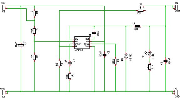
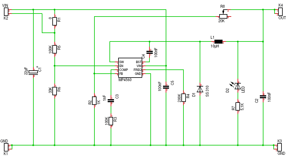
ausrechne komme ich auf knapp 300V pro Ausgang Das würde mich sehr wundern, da die Freilaufdiode SS310 nur 100V aushält, auch die Bezeichnung auf dem Mosfet 15N10 steht üblicherweise für 15A, 100V. > Meine Frage wäre was ich in die Platine an Spannung und Strom geben > muss Rot=+ und schwarz
gewünschten Drehantrieb – auf Wunsch angebaut oder einzeln beigelegt. Belimo NEWS R K o m p le tte sS o rtim e n t: K u g e lh a h n e nu n dA n trie b e Motorisierte Regel-Kugelhahnen mit gleichprozentiger Kennlinie Kennlinie: gleichprozentig Rohranschlüsse: Innengewinde Zulässiger Druck: 4140 kPa (
CHARACTERISTICS Ta = 2° C PARAMETER SYMBOL CONDITION MIN. TYP. MAX. UNIT REMARK POWER SUPPLY VOLTAGE VDD −SS 2.5 3.3 3.6 V POWER SUPPLY VOLTAGE VCC −SS 2.7 3.3 3.6 V FOR LED DRIVER LOGIC HIGH INPUT VOLTAGE VIH H LEVEL 0.8*VDD VDD V NOTE (1) LOGIC LOW INPUT VOLTAGE VIL L LEVEL 0 0.2*VDD V POWER SUPPLY
input is V SS− 0.3 ⎯ 0.46 × VDD V 3 V ≤ V DD < 4.5 V Input “L” selected voltage ⎯ Port inputs if TTL V SS− 0.3 ⎯ 0.8 V input is selected INITX input pin V ILR INITX ⎯ V SS− 0.3 ⎯ 0.2 × V DD V (CMOS Hysteresis) MD_2 to V ILM MD_0 ⎯ V SS− 0.3 ⎯ V SS+ 0.3 V Mode input pins External clock in V ILXDS X0, X0A ⎯ V SS− 0.3 ⎯ 0.5 V “Oscillation mode” 88 MB91460D Series (VDD5 = AVCC5 = 3.0 V to 5.5 V,SS5 = AVSS5 = 0 V, A= −40 °C to TA(ma)) Pin
kHz F 2 GHz 2 kHz F 3.5 GHz R4131CN/DN ± 1 .5 d B o r le s s ± 2 .5 d B o r le s s ± 4 d B o r le ss R e sid u a l re sp o n se :0 0 d B m o r le ss: W h en term in ated at input. R4131A/B ATT 0 dB a n d irip u t 50 2 -.9 5 d B m o r less: R413'1C/D in p u t -9 8 d B m o r le ss: W h en term in ated
minderwertiger Stahl bei tiefen Temperaturen zu Sprödbruch" neigt. https://en.wikipedia.org/wiki/SS_John_P._Gaines https://de.wikipedia.org/wiki/Spr%C3%B6dbruch
praktisch nachzuprüfen. CFK ist seit sehr langer Zeit Teil des Flugzeugbaus. Bereits beim Airbus A310 von 1983 bestand das Seitenleitwerk daraus. Ebenso wird das Material für Propeller verwendet. Man hat also einige Erfahrung damit. Trotzdem gibt es natürlich Ausfälle und wird es geben. Man wird
Habe es mit einer SS310 versucht. Hatte nix anderes zum testen. Der Transistor sperrt zwar mit 0.2 V aber es liegen trotzdem 0.5 V am anderen Ende der Diode an wenn der Transistor leitet. Der Spannungsabfall *schwebend*
ORDER over 2 break polarity HOW TO ASSEMBLE 2 unim c basic switch modules unimec15___ + 16contacts310 3contacts unimec15___ + 16270 + 16300 + 16324 contacts contacts A 1 change 2 make 2 break 2 change 2 make and reverse B Part no: 1 5 4 C over contact contacts contacts over 2 break polarityc™ unimec
mode (PSS1 = 0 and PSS3 = 0), TC0, TC1 and TC3 share a 10-bit prescaler CPS310, But they have different frequency settings. In single mode (PSS1 = 1 and PSS3 = 0), TC1 independently uses a 10-bit prescaler CPS1, TC0 and TC3 Share a 10-bit prescaler CPS310, but they have different
famous formula for the energy density of a black body. 0.60 0.50 0.40 Temperature: T = u(λ) [J 0.30 310 [K] m ] Replot 0.20 0.10 0.00 5 10 15 20 25 λ [μm] This plot was generated for an object with a temperture of 5700 K. That is the temperture of the surface of the sun. The peak in the spectrum is then
7908CT 1 A 312 Resistor 62 Q 4 A 301. R304 Resistor 100 c R31 9.R 320 , R325 Resistor 220 o 4 R 309, R 310 Resistor 470 n R 313, R 314 1 R 324 Resistor 1.2kU 1 R 318 Resistor 3.3 kQ 1 R 308 Resistor t.eec 1 R 322 Resistor 3 kU 1 R 315 ResistOf 3.9kO 1 R 321 Resistor 36kO 10 R307.R31 1.R316 Resistor 10kU
forBS. (Please refer to the Design Tip DT97-3 for more details). Note 2: When VDD< 5V, the minimumSS offset is limiteDD.o -V 2 www.infineon.com/gatedriver IR2110(S)PbF/IR2113(S)PbF Dynamic Electrical Characteristics VBIAS (VCC, VBS, DD ) = 15V, L = 1000 pF,AT = 25°C andSS = COM unless otherwise specified
7908CT 1 A 312 Resistor 62 Q 4 A 301. R304 Resistor 100 c R31 9.R 320 , R325 Resistor 220 o 4 R 309, R 310 Resistor 470 n R 313, R 314 1 R 324 Resistor 1.2kU 1 R 318 Resistor 3.3 kQ 1 R 308 Resistor t.eec 1 R 322 Resistor 3 kU 1 R 315 ResistOf 3.9kO 1 R 321 Resistor 36kO 10 R307.R31 1.R316 Resistor 10kU
in„ Channel FETage is negative / - v j i n Source Bias ResistV =R.-In so. R =—£. I- E s u 5 T _ \ T ss - 3 - 2 - 1 0 1 Currentwith set sourceR: Fig 2.18—Drain Current vs Source-to-Gate Voltage for J310 Fig 2.19—JFET bias circuit and equations. The left circuit is a type Junction Field Effect Transistor
irkt einen entsprechenden Ladestrom in den Blitzkondensator C 001. In der Primärwicklung 5/3 f lie ß t nun ein Strom, der sich zusammen s e tz t aus dem Laststrom (Sekundärstrom m u ltip liz ie rt mit dem Dber setzungsverhältnis von DA) und dem Magnetisierungsstrom des Trafos. Der Magnetisierungsstrom
2000 pF. 10 AGND Analog ground Internal reference for the regulator control functions Soft-start 11 SS An external capacitor and an internal 10 µA current source set the time constant for the rise of the error amp reference. The SS pin is held low during standby, Vcc UVLO and thermal shutdown. Output

 Bild
Bild

 Bild
Bild
 Bild
Bild