bit reference counter (R counter) allows Analog and digital lockdetect selectable REFIN frequencies at the PFD input. A complete Hardware and software power-down mode phase-locked loop (PLL) can be implemented if the synthesizer 104 MHzphase detector is used with an external loop filter and voltage controlled
Range T T -65 to +150 °C J, STG Notes: 1. No purposefully added lead. 2. Diode’s Inc.’s “Green” policy can be found on our website at http://www.diodes.com/products/lead_free/index.php. 3. Device mounted on FR-4 PC board with recommended pad layout, which can be found on our website at http://www.diodes.com
is available, a 10 kW/100 nF RC network temperature exceeds T SD . A Hysteresis prevents the part can be added between V IN and EN to delay the EN signal. from turning on until the die temperature cools atRSD. A logiclowonEN or high on EN turns-on the device. A logic Reverse Voltage Protection high
Ihrem Controller passenden Pin-Num- mern zu ermitteln. HINWEISE, TIPPS! Einige AVR-Controller (z.B. AT90CAN32/64/128, ATMega64/128) haben spezielle Programmierpins PDI, PDO. Bitte benutzen Sie diese Leitungen anstatt MISO/MOSI (siehe Datenblatt). ERFOS-AVR-ISP unterstützt die adaptive SPI-Bitratenanpassung
can refer to the figure as shown below. The output current can be kept constant regardless of the variations of LED forward voltages (V ). This peFforms as a perfection of load regulation. 100.00 90.00
Grayscalenstant−CurrentOUT15 Register 180 191 PWM−Control Driver 1CPRG Dx15y XERR DC−Register 6!Bit−Dot 90 95 0 Correction 191 DC−EEPROM 90 95 LED−Open−Detection SOUT VPRG 1 An IMPORTANT NOTICE at the end of this data sheet addresses availability, warranty, changes, use in safety-critical applications, intellectual
specified time. Note that occasional collisions are normal. 100 Mbps Green On The port is operating at 100 Mbps. The port is operating at 10 Mbps. Off Link Green On A valid link is established on the port. (located at the A link is not established on the port. top left corner Off of each vista 10BASE-T
and VVVF have no effect.AC output voltage is adjusted by the feedback resistor R23. This application can be used in as dimmer and voltage regulator. 2. In variable frequency and constant voltage mode (Pin VVVF at “0” low electrical level) 0~100Hz(FRQSEL1,FRQSEL0=10)or 0Hz~400Hz(FRQSEL1,FRQSEL0=11), pin
verfügbar. Die RS-Partnerfirma OKDO bietet die Platine mit 8 oder 16GB RAM an, die 8GB-Variante soll rund 90US-Dollar kosten. 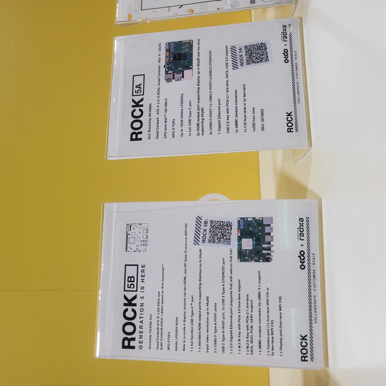 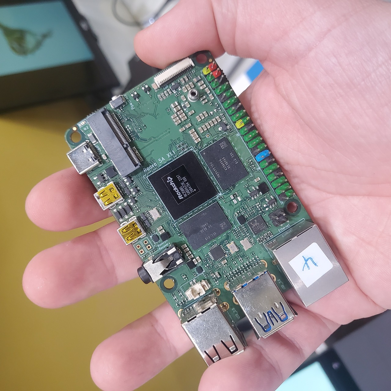 Der RockChip-Prozessor ist unter Anderem wegen seinem integrierten AI-Beschleuniger interessant – ob des neuen
LoRaWAN connectivity for terrestrial low power wide area networks (LPWAN) operating at 470MHz, 868MHz and 915MHz; it also provides LoRa 2.4GHz and the S-band for direct connection to satellites. [/c] In nicht allzu ferner Zukunft soll Murata ein mit diesem Prozessor ausgestattetes
rausgeschmissen wird. Auf Arbeit habe ich einen FTDI, der hat auch seine Macken. Bei den AVRs mit 64 Pins (AT90CAN128 usw.) liegt ja ISP und UART auf den selben Pins. Nach jedem Programmieren kackt der FTDI ab und das Terminalprogramm muß neu gestartet werden.
stg Soldering temperature(1) Tsld 260 °C Notes • Stresses in excess of the absolute maximum ratings can cause permanent damage to the device. Functional operation of the device is not implied at these or any other conditions in excess of those given in the operational sections of this document. Exposure to absolute maximum ratings for extended periods of the time can adversely affect reliability (1)Refer to reflow profile for soldering conditions for surface mounted devices. Also refer to “Assembly Instructions” (www.vishay.com/doc?80054) ELECTRICAL CHARACTERISTICS
" erfordert? Eine Übersicht der UDS CAN IDs wäre hilfreich, wie z.b.hier https://mk4-wiki.denkdose.de/artikel/can-bus/mk4_can-bus_modules
, mit "AT CAF0" die Protokollbehandlung abstellen und mit "AT H1" die Anzeige der CAN IDs einschalten. Gegebenenfalls auch noch mit "STCMM1" CAN ACKs beim Mitschneiden einschalten. Und dann startet man mit "STMA
be disabled. Available VBI lines are from line 6 to line 27 of both field 1 and field 2. Each line can be any VBI mode. Output data is available either through the VBI-FIFO (B0h) or through dedicated registers at 90h to AFh, 2 both of which are available through the I C port. 3.9 VBI FIFO and Ancillary
sehr > hilfreich. Dabei können neuere Studio-Varianten wenige AVR simulieren als früheren. Z.B. AT90CAN, -PWM und -USB kann man mit Stuio 4.19 simulieren, mit späteren aber nicht mehr. Glücklicherweise läuft Studio 4.19 auch mit Win11, das habe ich getestet. Beide (7 und 4.19) stehen nebeninander
components. The on-chip voltage regulator's primary purpose is to power the EFM32 USB PHY. But as it can deliver more current than the EFM32 needs, it can be used to power other components as well, even in non-USB applications. This can be very useful when component cost or PCB area is of concern. This
12.5 kHz On-line analysis of distortion, drift, modulation, and phase noise Dual-channel 6.25 kHz can benefit fromthespeed and accuracy ofthe HP 3562A. High reso- Amplitude lution measurements are typically 100 times faster than tuned spec- Accuracy: defined as full scale accuracy at any of the calcu
together with the additional load resulting from a routine weekly 10 s test, for at least 1 year before the battery fault warning is given. At the point when the battery fault warning commences, the batteries shall have sufficient capacity to give an alarm signal as specified in 5.17 for at least 4 min in the event of fire, or in the absence of fire a battery fault warning for at least 30 days. In the absence of suitable test procedures to verify battery capacity, data concerning the smoke
can refer to the figure as shown below. The output current can be kept constant regardless of the variations of LED forward voltages (V ). This peFforms as a perfection of load regulation. 100.00 90.00
NOTE o 0 GND OUTPUT Rating applies to ambient temperature up toe.0Above 70 e ambient derate linearly at 6.3mW /oC for Metal CanB.3mW/oC fo r DIP and 7mW/oC for the Flatpak. -1N NC +IN LAG v - LEAD EQUIVALENT CIRCUIT NC NC a V . ORDER INFORMATION TYPE PART NO. IlA702 IlA702DM R, + ---+ --'-0 LEAD p.A702C
steady IEC 60068-2-78, test Ca |△V/V (1 mA)| ≤10% state The specimen shall be subjected to 40 ±2 °C, 90 to 95 % r.H. for 56 days without load / with 10% of the Rinse100 M& maximum continuous DC operating voltage V . DC Then stored at room temperature and normal humidity for 1 to 2 h. Thereafter, the change
R1 and R2 should be selected carefully to ignore the SNS temperature coefficient of input current at the SNS pin.A EN current greater than 50μA in the resistor divider is GND recommended to meet the above requirement. The adjustable output voltage can be calculated using the Figure 5. FineAdjustable
Figure 36 when using the IC in an environment of Ta ≥ 25 °C. Even if the ambient temperature Ta is at 25°C, chip junction temperature (Tj) can be very high depending on the input voltage and the load current. Consider the design to be Tj ≤ Tjmax = 150 °C in whole operating temperature range. Should by
conductor indicator However, attention should be paid that the construction is suitable for UHF lane can be interrupted at the required posi tions, for instance with the aid 01 a sharp applications screwdriver. This board can be accommodat ed in a piece of 18 mm diameter copper water pipe. which can be
at the transistor DV 2880 have been used. They belong 10 a The residual VOltage U on can be calculated series 01 N·channel enhancement FETs thaI os comprise six types : DV 2805. DV 2810. DV 2820. wilh Ihe
drop as quickly. Second order stage has lower 1MD than the first. The in- products. If inputs occur at f ( and f 2 IMD can be a major difficulty in wide band designs, such as general coverage receiv- tercepts of each stage can be normalized to second order IMD occurs at frequencies any desired point in
Sascha schrieb im Beitrag #7355312: > CAN und LIN sind halbduplex, es kann also bei beiden Übertragungsarten > zu Buskollisionen kommen. Für CAN hat AVR-Serie AT90CAN32-128. Gibt es bei AVR etwas mit eingebauem LIN-Modul?
Maxim B. schrieb im Beitrag #7355331: > Sascha schrieb im Beitrag #7355312: >> CAN und LIN sind halbduplex, es kann also bei beiden Übertragungsarten >> zu Buskollisionen kommen. > Für CAN hat AVR-Serie AT90CAN32-128. Gibt es bei AVR etwas mit > eingebauem LIN-Modul? LIN ist
C 0 0 30 60 90 120 150 Output Current (mA) Figure 3-1. Quiescent Current vs Load Current for TLV704xx (New Chip Only) An IMPORTANT NOTICE at the end of this data sheet addresses availability, warranty, changes, use
the LOCAL command. Any variable created by LOCAL will vanish when the program leaves the subroutine. At its simplest level DIM and LOCAL can be used to define one or more variables based on their type suffix or the OPTION DEFAULT in force at the time. For example: DIM nbr%, s$ But it can also be used to
a reset. The BCLK signal can be output from BCLK pin by the BCLK output disable bit (bit 7 at address 0004 16) in the memory expan- sion and the microprocessor modes. The main clock division select bit 0(bit 6 at address 0006 16
change system properties ● Executes user-defined key sequences NOTE: The action key feature is enabled at the factory. You can disable this feature by pressing and holding the fn key and the left shift key. The fn lock light will turn on. After you have disabled the action key feature, you can still perform
of ROM: for booting and core functions • 320 KB of onchip SRAM: for data and instructions, running at a configurable frequency of up to 240 MHz. • RTC FAST Memory: 8 KB of SRAM in RTC. It can be accessed by the main CPU. It can retain data in Deep-sleep mode. • RTC SLOW Memory: 8 KB of SRAM in RTC. It
Offices For a current list of our domestic and international sales offices, go to the Lantronix web site at www.lantronix.com/about/contact . Disclaimer and Revisions Operation of this equipment in a residential area is likely to cause interference, in which case the user, at his or her own expense, will be
transmitting signal is less than 1%. In the Windows OS, after installing high-speed VCP vendor driver, it can emulate standard UART, so the mostly original serial applications are totally compatible, without any modification. CH348 can support up to 48-channel GPIO input and output function. CH348 can be used
Wettersatelliten Ringmischer-Baugruppe für den ATV-Sender nach DJ 4 LB Benno Rößle DJ 1 JZ 1981/2 85…90 Amateur- Fernsehen Ringmischer-Baugruppe für den ATV-Sender nach DJ4LB Benno Rößle DJ 1 JZ 1981/2 85…90 70-cm-Band Empfangskonverter für die geostatinären Wettersatelliten METEOSAT - GOES - GMS 1 Benno
Battery current consumption during - - 1.0 3.4 uA normal operation Battery current consumption during At 20℃ *Note2) - 30 35 uA back-up operation *Note1) The voltage value at the power terminal on the encoder. *Note2) The value when the axis is stopped and battery is 3.6[V]. S5094873B-6/22 5.3ElectricalSpecificationsforSingleTurn
TXS, ACT#, etc. TNOW is the status indication pin that the serial port is transmitting data, which can be used to control the RS485 transceiver switching. When TNOW outputs low or high level, UART sending and receiving can be performed at the same time. SUSPEND# and SUSPEND are the output signals to
Fernsehen Amateur- Ringmischer-Baugruppe für den ATV-Sender nach DJ 4 LB Benno Rößle DJ 1 JZ 1981/2 85…90 Fernsehen Ringmischer-Baugruppe für den ATV-Sender nach DJ4LB Benno Rößle DJ 1 JZ 1981/2 85…90 70-cm-Band Extrem rauscharmer 96-MHz-Quarzoszillator für die UHF/SHF-Frequenz- Bernd Neubig DK 1 AG 1981
fänger Wilfried Hercher DL 8 MX Eine quarzstabile Quelle für 10,37 GHz Jochen Jirmann DB 1NV 1985/2 90…96 Oszillatoren Eine quarzstabile Quelle für 10,37 GHz Jochen Jirmann DB 1NV 1985/2 90…96 3-cm-Band Ein V/D-D/A-Wandler für Video-Anwendungen Jochen Jirmann DB 1NV 1986/2 126 Sonstiges Neues zu aktiven
and CV to 0.05C cut off 2000 times Discharge: 1C discharge to 2.0V 80% or more of 1 cycle capacity at 1C discharge of operation Battery cell stored atC with 50% SOC 1Month 3Month 6Month Storage 4 Performance Cap Retention 90% 85% 80% Cap Recovery 95% 90% 85% 5 Initial Impedance Internal resistance measured
the data file(s) needs to be programmed. 6. Any memory location can be verified by using the Read instruction which returns the content at the selected address at the serial output MISO (PB1) pin. 7. At the end of the programming session, RESET can be set high to commence
are at 25°C and represent the most likely norm. (3) External components such as the catch diode, inductor, input and output capacitors can affect switching regulator system performance. When the LM2596 is used
thresholds. The SD pin is internally clamped with a 1 kΩ resistor and an 8 V zener clamp. The voltage at the SD pin should never exceed 14 V. If the voltage at the SD pin exceeds 8 V, the bias current will increase at a rate of 1 mA/V. The SD pin can also be used to implement various remote enable and disable
recirculation (90 bhp) - Misfiring - Injection commencement control - Charge pressure control - Automatic transmission - CAN bus 175_023 - Diesel direct injection system control unit - All sensors and actuators affecting
