#7852753: > Das dürfte ein 0,25W Widerstand sein. Der Eingebaute hat mit Sicherheit mehr als 1/4 Watt. Denke entweder 1 oder 2 Watt. Der hängt direkt an 320 V.
Widerstand wird bei einer Belastung > von 0,7 Watt zu warm. Natürlich, weil der 2 Watt Typ dann nur 0,35 Watt abführt? Merkst Du was?
DMAX 22 A Ta=-20 to +125°C (3) Single pulse AvalancheEnergy 1−2 EAS 500 mJ V = 30V, L=50mH DD ILpeak.4A Control Power SupplyVoltage 4−3 V 35 V CC SS/OLP pin Voltage 5−3 V V SSOLP −0.5~6.0 FB pin Inflowing Current 6−3 IFB 10 mA FB pin Voltage 6−3 V FB −0.5~9.0 V Within FBcontrol OCP/BD pin Voltage 7−3
Energy EAS Single pulse, DD = 30 V, L = 50 mH, Lpeak 4.4 A 500 mJ Input Voltage for Controller (MIC) VCC 35 V SS/OLP Terminal Voltage V SSOLP –0.5 to 6.0 V FB Terminal Inflow Current IFB 10 mA FB Terminal Voltage VFB IFBwithin the limits FB I –0.5 to 9.0
Schönheitsfehler aber egal. Eine Umformung in verständlichen Text geht z.B. so: >>> x=b'\x31\x32\x33\x34\x35\x36\x37\x38 >>> print (x) b'12345678' >>> print("".join("\\x%02x" % i for i in x)) \x31\x32\x33\x34\x35\x36\x37\x38 MeinAbschnitt. hier steht dann das blabla Punkt1 Punkt2 Punkt3 hmm, denkbar einfach
:2px;border-right:1px;"background-color:#FCD5B4" align="right"|Z C h jkl sortierbar. Um sortierbare Tabellen zu erhalten fügt man statt class="wikitable" folgendes ein: class="wikitable sortable". + Tabellen-Überschrift Überschrift links Überschrift
teil-Reparaturen bei AEG SVS Power Supply Systems GmbH durch- zuführen. S I C H E R H E I T S H I N W E I S E 4 Inhaltsverzeichnis ➜ Sicherheitshinweise 2 ➜ Sicherheitsbestimmungen 7 ➜ Hinweise zur vorliegenden Betriebsanleitung und Thyro-A 10 ➜ 1. Allgemeines 12 ➜ 2. Blockschaltbild 13 ➜ 3. Technische
hinterlegten Wert von 50µs ist. Empfohlenes Timing (Details hier) : Zeit High Zeit Low Kodierung "0" 0.35 µs ±150 ns 0.9 µs ±150 ns Kodierung "1" 0.9 µs ±150 ns 0.35 µs ±150 ns Reset - >50 µs (ab V4 >280µs) Die Gesamtdauer eines Bits beträgt 1.25 µs. Da das WS2812 Protokoll keinen gängigen Standards folgt
ATTiny817. Forenthread Entkoppelkondensator. Der laut Datenblatt vorgesehene Abblockkondensator von 100 nF ist unbedingt notwendig! Ohne diesen verhalten sich die LEDs fehlerhaft. Siehe auch. Forumsbeitrag: WS2812 funktioniert nach Anschluß von 100nF Forumsbeitrag: Signale an intelligenten LEDs (WS2812B)
folgenden Informationen für den Aufbau einers benutzerdefinierten Sensors. Sondengröße A Bestellnummer A = 4 5 6 8 x Passend für Schraubengröße M4 M5 M6 M8 Optional Schraubengröße Sondenkabellänge L Bestellnummer L = 5 10 15 20 23 25 30 35 40 45 x Länge in mm +/- 5 mm 50 100 150 200 230 250 300 350 400 450
HDR mode 1 N 0x22 Broadcast ENTHDR2 Enter HDR mode 2 N 0x23 Broadcast ENTHDR3 Enter HDR mode 3 N 0x24 Broadcast ENTHDR4 Enter HDR mode 4 N 0x25 Broadcast ENTHDR5 Enter HDR mode 5 N 0x26 Broadcast ENTHDR6 Enter HDR
SET FORTH AT www.vishay.com/doc?91000 TCND5000 www.vishay.com Vishay Semiconductors i 1.2 i s 1.0 n S a 0.8 t e p 0.6 e i l 0.4 e - e0.2 )r ( S 0 750 850 950 1050 1150 12786 λ- Wavelength (nm) Fig. 11 - Relative Spectral Sensitivity vs. Wavelength 0° 10° 20° 30° n i e i 40° e n l e 1.0 s e D t 0.9 50° r l u R 0.8 60° n -l A r 70° - S 0.7 ϕ 80° 0.6 0.4 0.2 0 94 8248 Fig. 12 - Relative Radiant Sensitivity vs. Angular Displacement t 1.0 e r Media: Kodak Gray Card u 0.8 I = 10 mA t F g L e 0.6 r v e 0.4 l e - 0.2 r r I
1 2 3 4 5 6 7 8 +3.3V +3.3V A 0 0 A 1 9 k 1 1 C39 V+ D1 R R 4 O D N1 STM32G051 6 CSB D V 100n MIC5236-3.3 +3.3V V SCL 2 SCK X2:2 2 IN OUT 3 4 VDD INT 7 L1 SDA 4 SDI 4 EN ERR 1 F.B.,0.2A 4 5 SDO 1 C3 C12 * C11
gemessen mit 10k/100nF/17V BC546B ok (6 ... 9V) KN2222A ok (4.9 ... 7.2V) CTBC546C ok (7.7 ... 11V) SF826C still @9V SC239E still @9V BC556B still @8V BC557B still @11V KN2907 still @10V SMD 2N2222A still @8V
Uwe (uhi) >gemessen mit 10k/100nF/17V >BC546B ok (6 ... 9V) >KN2222A ok (4.9 ... 7.2V) >CTBC546C ok (7.7 ... 11V) Ähm .. ich fände es super, auch die Frequenz hin zu schreiben. Das könnte später hilfreich sein.
Series 213 Series 215 Series UNIT Min Max Min Max Min Max Static Drain - Source VGS V =BS, I =1DµA 35 30 V(BR)DS Breakdown Voltage VGS V =BSV, I =D0 nA 30 10 10 20 Source - Drain V V = V =-5V, I =10 nA 22 10 10 20 Breakdown Voltage (BR)SD GS BD S Drain - Substrate VGB0V, I D 10nA V Breakdown Voltage V(BR)DBO SourceOpen 35 15 15 25 Source - Substrate V(BR)SBO VGB0V, I s10µA 35 15 15 25 Breakdown Voltage Drain Open Drain – Source VDS 10V 0.4 10 10 Leakage IDS(off) VGS V BS5V VDS 20V 0.9 10 Source - Drain I V = V =-5V VSD
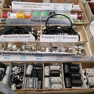
Měděný cínovaný vodič (drát) ø0,4 mm civka 25 m 50 Kč ø0,6 mm civka 15 m 50 Kč Kabely BNC BNC konektor s kabelem 20 Kč NC kabel 75 Ω 0,5 m 35 Kč N konektor na kabel 85 Kč 95 Kč 150 Kč Adaptery TNC N konektor 65 Kč feritový filtr na kabel 4-7 mm 20 Kč 7 mm 22 Kč 6-9 mm 25 Kč 11 mm 32 Kč 10-13 mm 36 Kč
MM74C02, MM54C00/MM74C00, MM54C04/MM74C04 MM54C02/MM74C02, MM54C04/MM74C04 AN006022-3 (a) AN006022-4 (b) AN006022-5 (c) FIGURE 3. Propagation Delay for 74C Gates The following three special cases may be useful. Figure 4 illustrates the approximate output waveform and the voltage V1at the charging node
2N7000 2N7002 N-channel 60 V, 1.8 Ω, 0.35 A, SOT23-3L, TO-92 STripFET™ Power MOSFET Features 2N7000 V60 V < 5 Ω(@10V) 0.35 A 3 2N7002 60 V < 5 Ω(@10V) 0.20 A 2 s ) ■ Low Qg 1 c t( ■ Low threshold drive
Min Max Min Max 74HC175 V IH HIGH-level V CC = 2.0 V 1.5 1.2 - 1.5 - 1.5 - V input voltage V CC = 4.5 V 3.15 2.4 - 3.15 - 3.15 - V V CC = 6.0 V 4.2 3.2 - 4.2 - 4.2 - V V IL LOW-level V CC = 2.0 V - 0.8 0.5 - 0.5 - 0.5 V input voltage V = 4.5 V - 2.1 1.35 - 1.35 - 1.35 V CC V CC = 6.0 V - 2.8 1.8 -
Typ Max Min Max Min Max 74HC138 VIH HIGH-level VCC = 2.0 V 1.5 1.2 - 1.5 - 1.5 - V input voltage V = 4.5 V 3.15 2.4 - 3.15 - 3.15 - V CC VCC = 6.0 V 4.2 3.2 - 4.2 - 4.2 - V VIL LOW-level VCC = 2.0 V - 0.8 0.5 - 0.5 - 0.5 V input voltage VCC = 4.5 V - 2.1 1.35 - 1.35 - 1.35 V V = 6.0 V - 2.8 1.8 - 1.8
T amb = -40 °C to +85 °C T amb = -40 °C Unit to +125 °C Min Typ [1] Max Min Max t transition time nQ, nQ; see Fig. 7 [3] VCC = 4.5 V - 7 19 - 22 ns W pulse width nCP HIGH or LOW; see Fig. 7 VCC = 4.5 V 23 9 - 27 - ns nSD, nRD LOW; see Fig. 8 VCC = 4.5 V 20 9 - 24 - ns rec recovery time nSD, nRD; see Fig. 8 VCC = 4.5 V 8 1 - 9 - ns su set-up time nD to nCP; see Fig. 7 VCC = 4.5 V 15 5 - 18 - ns t hold time nD to nCP; see Fig. 7 h VCC = 4.5 V 3 -3 - 3 - ns max maximum nCP; see Fig. 7 frequency VCC = 4.5 V 22 54
Max Min Max Min Max 74HC11 V IH HIGH-level V CC = 2.0 V 1.5 1.2 - 1.5 - 1.5 - V input voltage V = 4.5 V 3.15 2.4 - 3.15 - 3.15 - V CC V CC = 6.0 V 4.2 3.2 - 4.2 - 4.2 - V V IL LOW-level V CC = 2.0 V - 0.8 0.5 - 0.5 - 0.5 V input voltage V CC = 4.5 V - 2.1 1.35 - 1.35 - 1.35 V V CC = 6.0 V - 2.8 1.8
DC Forward Current Figure 8: Maximum Forward Current vs. Ambient Temperature 1.2 35 d c A m 1.0 m30 Y - I A N S m E25 E 20.8 R T T U I A C20 S D0.6 D O I E I L L15 M A A L R0.4 W E O O10 I ( L T 0.2 A L X 5 E M R 0.0 0 0 5 10 15 20 25 30 0 10 20 30 40 50 60 70 80 90 FORWARD CURRENT-
Temperature 100 20 90 SCL = 100 kHz VCC = 2.5 V All I/Os unloaded 18 ) 80 16 TA= −40ºC A ( 70 ) 14 n A T = 25ºC e 60 ( 12 A u 50 N 10 C I p 40 8 p S 30 6 20 4 TA= 85ºC 10 2 0 0 2.0 2.5 3.0 3.5 4.0 4.5 5.0 5.5 0.0 0.1 0.2 0.3 0.4 0.5 0.6 Supply Voltage (V) Vol (V) Figure 4. I/O Sink Current vs Output
/ 5.5 V) 4 m t set-up time for STOP condition 4.0 - 0.6 - 0.26 - μs p n SU;STO i s tBUF bus free time between a STOP and 4.7 - 1.3 - 0.5 - μs 2 b 1 t START condition 4 l C capacitive load for each bus line [10]
drawings, please see the Microchip Packaging Specification located at http://www.microchip.com/packaging 4X ș1 R1 H R c SEATING PLANE C L ș (L1) 4X ș 1 DETAIL B Units MILLIMETERS Dimension Limits MIN NOM MAX Number of Terminals N 8 e Pitch 0.65 BSC Overall Height A – – 1.10 Standoff A1 0.00 – 0.15 Molded
V CC= 0.1% THD+N from 20Hz–20kHz. ±28V The performance of the LM3886, utilizing its Self • 50W Cont. Avg. Output Power into 8Ω at V CC= Peak Instantaneous Temperature (°Ke) (SPiKe) ±35V protection circuitry, puts it
latchup prot OHμC IH GND IHmax Calculation example: For VCCpeak = -100V; Ilatchup≥ 20mA; V OHμC ≥ 4.5V 5kΩ ≤ R prot≤ 65kΩ. Recommended values: R = 10kΩ, C = 10nF . prot EXT Doc ID 15994 Rev 5 25/37 Application information VN5E016AH-E 3.4 Current sense and diagnostic The current sense pin performs a
0 5 6 B 3 4 C C 4 3 A---------V 42R +51C 02D Ω74 5 6 Fu022 4 + - V61 8 k 05 4 kΩ B Fu1.0 4 F . R R 1 2 K K 5 4 2 35C 1 61D 1 3 2 Ω Ω 2 6 R . 6 R 9 U 45R 0 C R 5 5 R 9 4 1 4 K 4 5 M 5 C C 0 R 5 L 7 Ω001 1AC 71D 14R
temperature specified above for curves A and B. 25/34 Package and PC board thermal data VND5E160J-E 4 Package and PC board thermal data 4.1 PowerSSO-12 thermal data Figure 35. PowerSSO-12 PC board Note: Layout conditionthf R thd Z measurements (PCB: Double layer, Thermal Vias, FR4 area= 77mm x 86mm,
OUT> OL STATUSOLTAdEun VOL ro e P OPEN LOAD without external pull-up le t INPUTn s o LOAD VOLTAGE n O b STATUS n T OVERTEMPERATURE Tj TRSD INPUn LOAD CURRENT n STATUS n 12/27 Doc ID 9431 Rev 5 VND830LSP Electrical specifications 2.4 Electrical characteristics curves Figure 7. Off-state output current
single-sided FR-4 board with 0.5 cm of Cu (at least 35 µm thick). Horizontal mounting and 2. When mounted on a standard single-sided FR-4 board with 6 cm of Cu (at least 35 µm thick). Horizontal mounting and no artificial
on FR4 printed circuit board with 0.5 cm of Cu (at least 35 µm thick). 2. When mounted on FR4 printed circuit board with 6 cm of Cu (at least 35 µm thick). Doc ID 10896 Rev 4 7/27 Electrical specifications
voll Thorsten S. schrieb im Beitrag #7846954: > belastet ca. 30V > DC Ja, hier nur 1/4, aber die volle Spannung von 8x40 V wird sicher lange nicht erreicht, aber deswegen ja anfangs auch die Frage hier.
von der Seite 8:52 149 V DC Etwas Schatten / Seitliche Sonnenstrahlen 9:04 178 V DC Ost Sonne auf 4 Modulen voll, 4 teilschatten 9:09 190 V DC 9:12 202 V DC Jetzt ist die Röhre langsam am Punkt. >>33000 lux 5A 265V 1325W kritisch Schalte gleich ab. Michael B. schrieb im Beitrag #7848020:
composition see 70 °C 85 °C 85 °C max max MOQ below) 10 kHz 10 kHz 10 kHz 1 kHz 10 kHz µF mm mm A A m nH 10-3 10-3 V = 900 V DC, V = 720 V DC R,85 °C op,100 °C 35.0 30.0x45.0x57.5 20.3 B32718H9356+000 18.2 15.8 5.8 14.5 2.3 22.7 280 45.0 35.0x50.0x57.5 20.3 B32718H9456+000 21.3 18.5 4.9 16.0 2.4 23.0 108
Hallo, habe hier ein defektes AsRock 990FX Extreme4 eines Bekannten der auf die tolle Idee gekommen ist die dicke Schutzfolie (roter Pfeil) auf dem Kühlkörper mit dem A nicht zu entfernen. Die dicke Folie war Jahre auf dem Kühlkörper und jetzt funktioniert
schrieb im Beitrag #8069334: > Weshalb doppelt? Damit die Suchmaschinenbots wat zu tun ha'm -Schö'n Freidach
Die als rechtliche Infrastruktur dienende ThreadX Alliance ist nun startbereit, mit der Version 6.4.2 steht das erste ohne MS-Mitarbeiter zusammengestellte Release am Start. Im Bezug auf die Zertifikation von 6.4.x war die aktuelle Aussage, dass der von Microsoft bekannte Abdeckungslevel gegen Ende
zu wildern sucht: [c] Utilizing the 2.4GHz and 5GHz Wi-Fi frequency bands, the FCM363X boasts a high-performance ARM Cotex-M33 processor clocked up to 260MHz and features built-in 1.2MB SDRAM and 8MB flash memory. PSRAM is also supported

 Bild
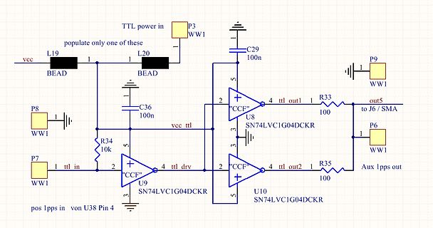
 Bild
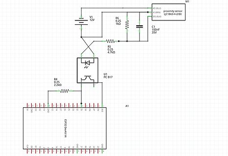
 Bild
 Bild
 Bild
 Bild
 Bild