-
 Bild
Bild
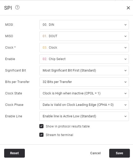
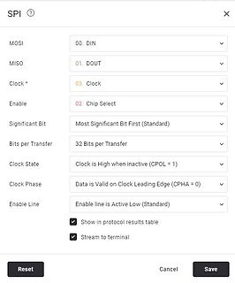
SPI Konfigurationsmenü einer Software
03. Clock Enable 02. Chip Select Significant Bit Most Significant Bit First (Standard) Bits per Transfer 32 Bits per Transfer Clock State Clock is High when inactive (CPOL = 1) Clock Phase Data is Valid on Clock Leading Edge (CPHA = 0) Enable Line Enable line is Active Low (Standard) Show in protocol
in „C > Anzahl an Words von übergebenen Bytes berechnen?“ · Mikrocontroller und Digitale Elektronik · · Screenshots
-
PDF
TLP293_4_datasheet_en_20190520.pdf
production 2014-04 © 2019 Toshiba Electronic Devices & Storage Corporation 1 2019-05-20 TLP293-4 Current Transfer Ratio (Unless otherwise specified, Ta=25°C) Current Transfer Ratio (%) Rank Test condition Marking of Classification (Note 1) C / F Min Max Blank 50 600 Blank F = 5 mA, CE = 5 V GB 100 600 GB LA (
in „Optokoppler TLP293-4 - Datenblatt lesen“ · Mikrocontroller und Digitale Elektronik ·
-
PDF
73758.pdf
transmission between circuits of different po- 1. 4pin DIP package tentials and impedances 2. Double transfer mold package (Ideal for Flow Solder- ing) 3. High collector-emitter voltage (V CEO:80V )*) 4. Current transfer ratio (CTR : MIN. 50% at I F5 mA, V CEV) 5. Several CTR ranks available 6. High isolation
in „PC817 Hilfe wiederstände bestimmen“ · Analoge Elektronik und Schaltungstechnik ·
-
PDF
ADUC7019_7020_7021_7022_7024_7025_7026_7027_7028.pdf
Table 60. SPICON MMR Bit Descriptions Bit Description Function 15:13 Reserved. – 12 Continuous Transfer Set by user to enable continuous transfer. In master mode, the transfer continues until no valid data is Enable. available in the TX register. CS is asserted and remains asserted for the duration of each 8-bit serial transfer until TX is empty. Cleared by user to disable continuous transfer. Each transfer consists of a single 8-bit serial transfer. If valid data exists in the SPITX register, then a new transfer is initiated
-
PDF
DEM16216.pdf
Read) R/W = 0 (Write) 6 E Read/Write Enable Signal 7 DB0 8 DB1 9 DB2 Bi-directional data bus, data transfer is performed once, thru 10 DB3 DB0 to DB7, in the case of interface data. Length is 8-bits; and 11 DB4 twice, thru DB4 to DB7 in the case of interface data length is 4- 12 DB5 bits. Upper four bits
in „LCD Ansteuern mit PIC 16F84A funzt nicht“ · Mikrocontroller und Digitale Elektronik ·
-
PDF
sdphysical_simplifyed_Ver101.pdf
line. Data transfer can be configured by the host to use single or mul- DO Date: April 2 001 (c)2001 b y SD Group (MEIASanD10k,Toshiba) Simplified Version SD-Memory Card Specifications / Part 1. Physical Layer Specification; VersiSD Memory Card System Concept to card to host datto hostcard stops data transfer CMD command response command response DAT block read operationck crc data block crc data block data stop operation multiple block read operation Figure 5: (Multiple) Block read operation data line
-
PDF
-btspeaker.cn-OVC3860_RevE_AT_Command_Guide_v1.1.pdf
Redialing Redial the last outgoing call: AT#CH return: IC /* Call-setup status is outgoing */ ➢ Audio transfer Transfer audio between HSHF and phone speaker: AT#CO when transfered to HSHF, ovc3860 returns: MC /* The voice is on Bluetooth indication */ when transfered to HSHF: MD /*The voice is on phone indication
in „A2DP Bluetooth Modul China eBay“ · HF, Funk und Felder ·
-
PDF
BLK-MD-SPK-B_AT_Commands_OVC3860_List__1_.pdf
Redialing Redial the last outgoing call: AT#CH return: IC /* Call-setup status is outgoing */ ➢ Audio transfer Transfer audio between HSHF and phone speaker: AT#CO when transfered to HSHF, ovc3860 returns: MC /* The voice is on Bluetooth indication */ when transfered to HSHF: MD /*The voice is on phone indication
in „Adruino nano und Bluetooth chip OVC3860, Bei Anruf LED an und beim Auflegen LED aus“ · Mikrocontroller und Digitale Elektronik ·
-
PDF
MOSFET_Switched_Mode_Amplifiers_Part_1_-_Handimans_Guide.pdf
MeettheMOSFET current and heating of the mosfet – and them at 7MHz or higher. I faxed them the "transfer characteristics" of a often failure. If you haven't blown up an device, as illustrated in Fig. 1A, MOSFET's have been used for years in IRF510 yet – you just haven't worked some QRP circuits to prove
-
PDF
MC9S08DZ60_Data_Sheet.pdf
on CCR s e d n l Source Operation Description r d o r y Form d o p e C V H I N Z C A M O O s B Transfer Accumulator to TAP CCR CCR ← (A) INH 84 1 TAX Transfer Accumulator to X ← (A) – – – – – – INH 97 1 X (Index Register Low) Transfer CCR to – – – – – – TPA Accumulator A ← (CCR) INH 85 1 TST opr8a (
in „Bei AD-wandlung Bitsverlust“ · Mikrocontroller und Digitale Elektronik ·
-
PDF
MC9S08DZ60.pdf
CCR); SP ← (SP) – $0001 I ← 1; PCH ← Interrupt Vector High Byte PCL ← Interrupt Vector Low Byte Transfer Accumulator to CCR TAP CCR ← (A) INH 84 1 p ↕ 1 1 ↕ ↕ ↕ ↕ ↕ Transfer Accumulator to X (Index Register TAX Low) INH 97 1 p – 1 1 – – – – – X ← (A) TPA Transfer CCR to Accumulator INH 85 1 p – 1 1 –
in „Delay Funktion für Freescale“ · Mikrocontroller und Digitale Elektronik ·
-
Datei
atmel-bug.diff
:09:45.485390288 +0100 @@ -205,7 +205,7 @@ } else // else { - write_SPI(MM_PAGE_TO_B2_XFER); // transfer next page to buffer1 + write_SPI(MM_PAGE_TO_B1_XFER); // transfer next page to buffer1 } write_SPI((char)(page_counter >> 6)); write_SPI((char)(page_counter << 2));
in „AVR SoundRecorder“ · Mikrocontroller und Digitale Elektronik ·
-
Datei
USI_SPI.c
#include <avr/io.h> #include <avr/interrupt.h> #include <util/delay.h> unsigned char SPI_transfer(unsigned char data) { USIDR = data; USISR = (1<<USIOIF); USICR = (1<<USIWM0)|(1<<USICS1)|(1<<USICLK)|(1<<USITC); while (!(USISR & (1<<USIOIF))) { USICR |= (1<<USITC) ; } return USIDR; } int main (void) { DDRA = (1<<PA4)|(1<<PA5); sei(); while(1) { SPI_transfer(0xAA); PINA |= (1<<PA5); _delay_us(10); } }
in „µC hängt bei SPI über USI“ · Mikrocontroller und Digitale Elektronik ·
-
PDF
ST7066U.pdf
MPU Starts data read/write. Four high order bi-directional tristate data bus pins. Used for data transfer and receive DB4 to DB7 4 I/O MPU between the MPU and the ST7066U. DB7 can be used as a busy flag. Four low order bi-directional tristate data bus pins. Used for data transfer and receive DB0 to DB3
in „LCD Zeichensatz wechseln?“ · Mikrocontroller und Digitale Elektronik ·
-
PDF
MP600_DataSheet.pdf
Device Controller support several endpoints for communication with USB Host. - Control Read/Write transfer - Interrupt Transfer - Downstream Bulk Transfer from Host - Upstream Bulk Transfer to Host - Upstream Video Isochronous /Bulk Transfer to Host - Upstream Audio Isochronous /Bulk Transfer to Host The upstream bulk or isochronous transfer is accomplished with DMA operation. 4.9 Digital Audio Interface Unit (AIU) The Digital Audio Interface Unit (AIU) handles data communication between MP600 and internal/external audio CODEC. Both audio
in „Datenblatt von Magic Pixel MP600BUCG“ · Mikrocontroller und Digitale Elektronik ·
-
PDF
ST7066U.pdf
MPU Starts data read/write. Four high order bi-directional tristate data bus pins. Used for data transfer and receive DB4 to DB7 4 I/O MPU between the MPU and the ST7066U. DB7 can be used as a busy flag. Four low order bi-directional tristate data bus pins. Used for data transfer and receive DB0 to DB3
in „LCD- Das ewige Leiden“ · Mikrocontroller und Digitale Elektronik ·
-
PDF
BMA150_DataSheet_Rev1.4_14Jan2008.pdf
change without notice. Data sheet BMA150 Bosch Sensortec Triaxial, digital acceleration sensor Data transfer begins by a falling edge on SDA when SCK is high (start condition (S) indicated by I²C bus master). Stop condition (P) is a rising edge on SDA when SCK is high (see figure 12). Bit transfer: One data
-
PDF
MCS51LB.pdf
innerhalb des aktuellen 2KB-Blocks zur Verfügung. Sonder-Befehle: Für spezielle Aufgaben. 5.1.1 Transfer-Befehle MOV = MOVe = Bewegen Mit Transfer-Befehlen werden Daten zwischen den Komponenten des Mikrocontrollersystems ausgetauscht. Es existieren Befehle zum Datenaustausch innerhalb des Mikrocontrollers
in „MCS51-Kurs sinnvoll?“ · Mikrocontroller und Digitale Elektronik ·
-
Datei
ESP32_SPItest.ino
setHwCs(true); } void loop() { SPI1.beginTransaction(SPISettings(3000, MSBFIRST, SPI_MODE0)); SPI1.transfer16(0xA200); // Write 00 to R20 SPI1.endTransaction(); delay(1000); SPI1.beginTransaction(SPISettings(3000, MSBFIRST, SPI_MODE0)); SPI1.transfer16(0xA2ff); // Write 00 to R20 SPI1.endTransaction();
in „Frage zu SPI.beginTransaction“ · Mikrocontroller und Digitale Elektronik ·
-
PDF
TAS6424-q1.pdf
multiple-byte data transfers. 9.5.3 Random Write As shown in Figure 43, a single-byte data-write transfer begins with the master device transmitting a start condition followed by the I C device address and the R/W bit. The R/W bit determines the direction of the data 2 transfer. For a write data transfer
in „Eagle lib für TAS6424“ · Platinen ·
-
PDF
D2XXPG21.pdf
Intl. Ltd. 2002 Page 34 of 64 D2XX Programmer’s Guide 2.01 FT_SetUSBParameters Set the USB request transfer size. FT_STATUS FT_SetUSBParameters ( FT_HANDLE ftHandle, DWORD dwInTransferSize, DWORD dwOutTransferSize ) Parameters ftHandle Handle of the device. dwInTransferSize Transfer size for USB IN request. dwOutTransferSize Transfer size for USB OUT request. Return Value FT_OK if successful, otherwise the return value is an FT error code. Remarks Previously, USB request transfer sizes have been set at 4096 bytes
in „FTDI USB Programmierung mit C unter Linux“ · Softwareentwicklung ·
-
PDF
HD44780u_lcd2.pdf
write. DB4 to DB7 4 I/O MPU Four high order bidirectional tristate data bus pins. Used for data transfer and receive between the MPU and the HD44780U. DB7 can be used as a busy flag. DB0 to DB3 4 I/O MPU Four low order bidirectional tristate data bus pins. Used for data transfer and receive between the
in „LCD - Displaycode 4 Bitmodus“ · Mikrocontroller und Digitale Elektronik ·
-
PDF
HD44780.pdf
write. DB4 to DB7 4 I/O MPU Four high order bidirectional tristate data bus pins. Used for data transfer and receive between the MPU and the HD44780U. DB7 can be used as a busy flag. DB0 to DB3 4 I/O MPU Four low order bidirectional tristate data bus pins. Used for data transfer and receive between the
in „LCD-Anzeige-Problem“ · Mikrocontroller und Digitale Elektronik ·
-
PDF
hd44780.pdf
write. DB4 to DB7 4 I/O MPU Four high order bidirectional tristate data bus pins. Used for data transfer and receive between the MPU and the HD44780U. DB7 can be used as a busy flag. DB0 to DB3 4 I/O MPU Four low order bidirectional tristate data bus pins. Used for data transfer and receive between the
in „Reziproker Frequenzzähler+ Optimierte 64bit uint Routinen“ · Projekte & Code ·
-
PDF
AD7912_7922.pdf
passing through The measured ratio of signal-to-noise and distortion at the the endpoints of theADC transfer function.For theAD7912/ output of theA/D converter.The signal is the rms value of the AD7922,the endpoints of the transfer function are zero scale,a sine wave,and noise is the rms sum of all nonfundamental
in „Problem mit STM32 und AD7912“ · Mikrocontroller und Digitale Elektronik ·
-
PDF
STS7C4F30_STripFET.pdf
1350 pF Coss Output Capacitance VDS = 25V, f = 1 MHz, GS = 0 n-ch 250 pF p-ch 490 pF Crss Reverse Transfer n-ch 85 pF Capacitance p-ch 130 pF 2/10 STS7C4F30L ELECTRICAL CHARACTERISTICS (continued) SWITCHING ON Symbol Parameter Test Conditions Min. Typ. Max. Unit N-CHANNEL V = 15 V I = 3.5 A td(on) Turn-on
in „[S] STS7C4F30L StripFET“ · Markt ·
-
PDF
PWM-X.pdf
Forthe model PWM-X,the electronics switches between 24 predefined stagesaccordingto the following transfer curve Min PWM transfer charateristic 53% 25 0 10 20 30 40 50 60 70 80 90 100 20 % PW%PWM e The variantC/A hasbeen created especially for the boiler controller g15 e s type Honeywell MCBA14xxD-HR7A a e s w r P10 w o P 5 Transfer curve : PWM-C/A TransfercurvePWM-C/A 3,5 0 0 10 20 30 40 50 60 70 80 90 100 17% PWM [%] Max 3 PWM % MAX Type PWM-C Forthe model PWM-C,the electronic controlprovides one of the 3 2,5 hydraulic curvesof
in „[V] Wilo Pumpen mit externer PWM-Ansteuerung, RS15/6 PWM“ · Markt ·
-
Datei
LCD_library.txt
else pinChange(D7,0); } void Lcd8_Cmd(char a) { pinChange(RS,0); // => RS = 0 Lcd8_Port(a); //Data transfer pinChange(EN,1); // => E = 1 _delay_ms(1); pinChange(EN,0); // => E = 0 _delay_ms(1); } void Lcd8_Clear() { Lcd8_Cmd(1); } void Lcd8_Set_Cursor(char a, char b) { if(a == 1) Lcd8_Cmd(0x80 + b); else
in „LCD Initialisierung funktioniert nicht“ · Mikrocontroller und Digitale Elektronik ·
-
PDF
2SK1119_datasheet_en_20090929__1_.pdf
Applications Unit: mm z Low drain−source ON resistance : R = 3.0 Ω (typ.) DS (ON) z High forward transfer admittance : |Yfs = 2.0 S (typ.) z Low leakage current : IDSS = 300 μA (max) (V DS = 800 V) z Enhancement mode : Vth = 1.5 to 3.5 V DS = 10 V, D = 1 mA) Absolute Maximum Ratings (Ta = 25°C) Characteristics
in „brauche hilfe beim Nachbau eines DC-DC-Converters“ · Analoge Elektronik und Schaltungstechnik ·
-
PDF
SA_opto.pdf
OP1 Optional Optocoupler Analyzer The OP1 module allows the detection and the Current Transfer Ratio measurement of most standard optocouplers. The module without any component must be connected to the M3 before power-up. When the M3 is powered on, the module is recognizedby the tester and
-
 Bild
Bild
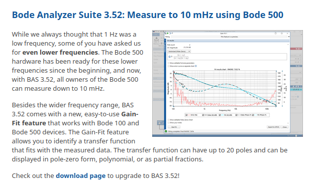
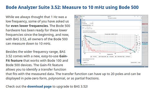
Werbetext für Bode Analyzer Suite 3.52 Software
feature that works with Bode 100 and Bode 500 devices. The Gain-Fit feature allows you to identify a transfer function that fits with the measured data. The transfer function can have up to 20 poles and can be displayed in pole-zero form, polynomial, or as partial fractions. Check out the download page to
in „ESP32-S31-Evaluationsboards, RISC/V-Benchmarks, neue Messtechnik und mehr“ · Mikrocontroller und Digitale Elektronik · · Screenshots
-
 Bild
Bild
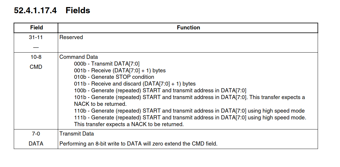
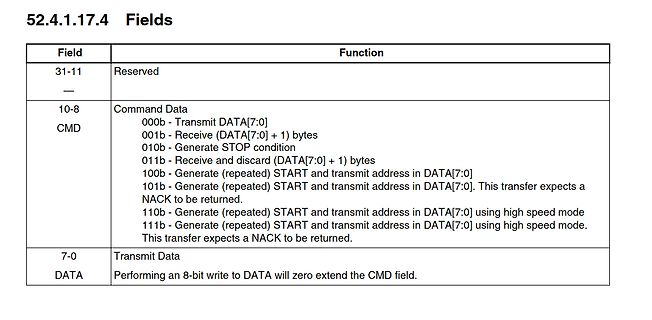
Tabelle mit Registerfeld-Definitionen
transmit address in DATA[7:0] 101b - Generate (repeated) START and transmit address in DATA[7:0]. This transfer expects a NACK to be returned. 110b - Generate (repeated) START and transmit address in DATA[7:0] using high speed mode 111b - Generate (repeated) START and transmit address in DATA[7:0] using high speed mode. This transfer expects a NACK to be returned. 7-0 DATA Transmit Data Performing an 8-bit write to DATA will zero extend the CMD field.
in „Induktiver Sensor antwortet nicht auf I2C“ · Platinen · · Screenshots
-
 Bild
Bild
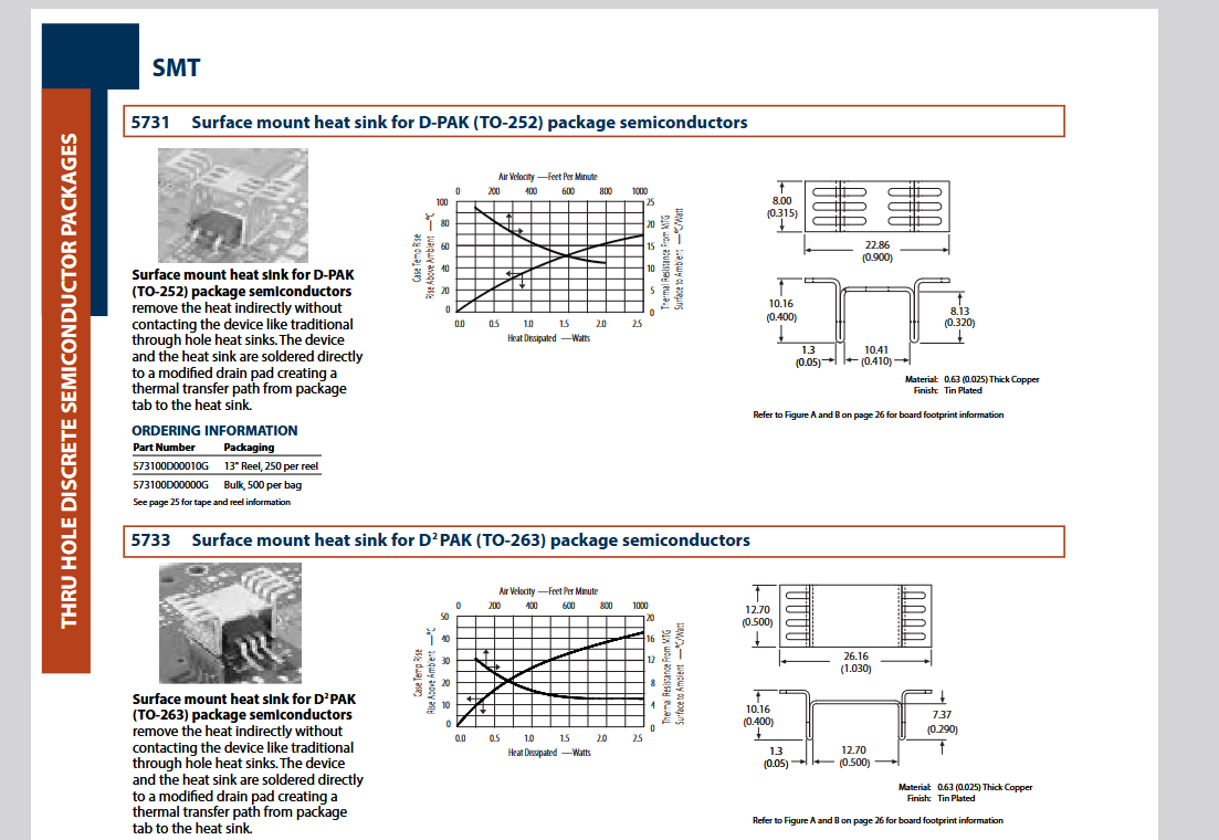
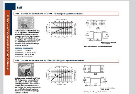
Datenblatt für D-PAK und D2-PAK Kühlkörper
hole heat sinks. The heat sink are soldered directly to a modified drain pad creating a thermal transfer path from package tab to the heat sink. ORDERING INFORMATION Part Number 5731010G 13" Reel, 250 per reel 5731000G Bulk, 50 per bag 5733 Surface mount heat sink for D2 PAK (TO-263) package semiconductors
in „schwebende Kühlkörper - normal?“ · Analoge Elektronik und Schaltungstechnik · · Screenshots
-
PDF
X1226.pdf
and • Alarm IRQ output 2 write operations. • 2-wire interface interoperable with I C —400kHz data transfer rate The clock/calendar provides functionality that is con- • Secondary power supply input with internal trollable and readable through a set of registers. The clock, using a low cost 32.768kHz crystal
in „kann RTC X1226 nicht beschreiben“ · Mikrocontroller und Digitale Elektronik ·
-
Datei
stm32f4xx_spi.c
in I2S mode or I2Sxext for I2S full duplex mode. * @param SPI_I2S_DMAReq: specifies the SPI DMA transfer request to be enabled or disabled. * This parameter can be any combination of the following values: * @arg SPI_I2S_DMAReq_Tx: Tx buffer DMA transfer request * @arg SPI_I2S_DMAReq_Rx: Rx buffer DMA transfer request * @param NewState: new state of the selected SPI DMA transfer request. * This parameter can be: ENABLE or DISABLE. * @retval None */ void SPI_I2S_DMACmd(SPI_TypeDef* SPIx, uint16_t SPI_I2S_DMAReq
in „GCC Optimierung killt Funktion“ · Mikrocontroller und Digitale Elektronik ·
-
PDF
DS2431-A1.pdf
the EEPROM 3 array are a two-step process. First, data is written to the Address Registers and Transfer Status scratchpad and then copied into the main array. This The DS2431-A1 employs three address registers: TA1, 1 allows the user to first verify the data written to the TA2, and E/S (Figure 6). These
in „Hardware Erkennung leicht gemacht“ · Mikrocontroller und Digitale Elektronik ·
-
PDF
AS5410_Datasheet_EN_v2.pdf
state after the Ready output has been set. Serial Interface (SPI) The SPI interface provides data transfer between AS5410 and the external microcontroller. Theminimumnumberofconnectionsbetweenmicrocontroller and AS5410 is three: 1. MOSI: Master Out – Slave In; data transfer from microcontroller to AS5410
in „SPI funktioniert nicht“ · Mikrocontroller und Digitale Elektronik ·
-
 Bild
Bild
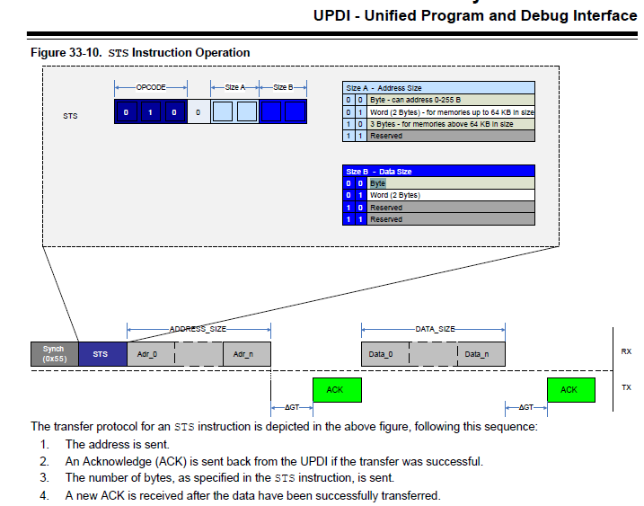
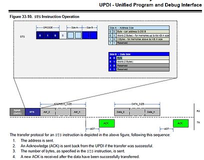
STS Instruction Operation Diagramm und Protokollsequenz
Reserved ADDRESS_SIZE DATA_SIZE RX Synch (0xSS) STS Adr_0 Adr_n Data_0 Data_n TX ΔGT ACK ΔGT ACK The transfer protocol for an STS instruction is depicted in the above figure, following this sequence: 1. The address is sent. 2. An Acknowledge (ACK) is sent back from the UPDI if the transfer was successful.
in „ATTiny3216 über UPDI Software-Reset auslösen“ · Mikrocontroller und Digitale Elektronik · · Screenshots
-
PDF
CPU08RM.pdf
Carry Bit SEC Set Interrupt Mask SEI Enable IRQ and Stop Oscillator STOP Software Interrupt SWI Transfer Accumulator to Condition Code Register TAP Transfer Accumulator to X (Index Register Low) TAX Transfer Condition Code Register to Accumulator TPA Test for Negative or Zero TSTA, TSTX Transfer Stack
-
 Bild
Bild
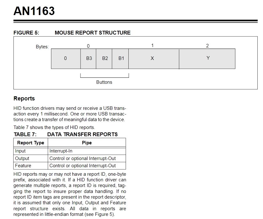
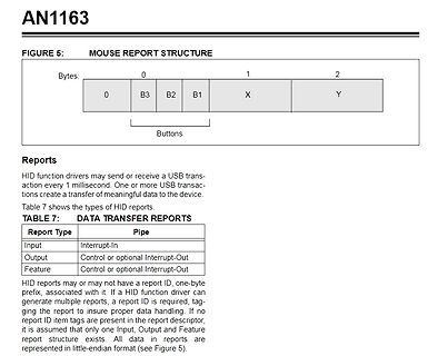
Ausschnitt aus einem Datenblatt zur Mouse Report Structure
send or receive a USB trans- action every 1 millisecond. One or more USB transac- tions create a transfer of meaningful data to the device. Table 7 shows the types of HID reports. TABLE 7: DATA TRANSFER REPORTS Report Type Pipe Input Interrupt-In Output Control or optional Interrupt-Out Feature Control
in „Bandbreite Bluetooth mouse“ · Mikrocontroller und Digitale Elektronik · · Screenshots
-
Datei
avrasm.txt
branch if same or higher (C = 0) nach Vergleich von Zahlen ohne Vorzeichen brtc label ; branch if transfer flag cleared (T = 0) brts label ; branch if transfer flag set (T = 1) brvc label ; branch if overflow flag cleared (V = 0) brvs label ; branch if overflow flag set (V = 1) bset 7 ; bit set in SREG register bst r0, 7 ; bit store in transfer flag (T flag bekommt Wert von Bit) cbi io31, 7 ; clear bit in IO-Register (nur untere 32 IO-Adressen) cbr r16, 255 ; clear bits in register (r16 AND 1-er Komplement von Konstante, Ergebnis in r16)
-
PDF
NL2432HC22-40J-NEC.pdf
Register R26 (R1Ah) 1st byte 2nd byte /CS SCL SI X X 0 X X X X 0 0 0 0 1 1 0 1 0 MSB LSB Specify to transfer of the resister number value at the next transfer Transfer of the resister number value 3rd b yte 4th byte /CS SCL SI X X 0 X X X X 1 0 1 0 1 0 1 0 1 MSB LSB Specify to transfer of the resister data Transfer of the resister data value value at the next transfer Note1: During 32-bit transfer of the Resister Data, /CS pin (Pin No.35) must be maintained active. Note2: "X" is set in accordance with the usage
in „TOMTOM DISPLAY“ · Mikrocontroller und Digitale Elektronik ·
-
Datei
ili9341.c
aux_spi_setClockDivider(bcm2835_aux_spi_CalcClockDivider(ILI_CLOCK)); bcm2835_aux_spi_setCS(2); (void)bcm2835_aux_spi_transfer(0x00); //Dummy read dont care about it char rxBuf[3] = { 0x00, 0x00, 0x00 }; bcm2835_aux_spi_transfern(rxBuf, sizeof(rxBuf)); bcm2835_gpio_write(RPI_BPLUS_GPIO_J8_36, HIGH); //CS High to end transmission
in „ILI9341 SPI Pixel auslesen geht teilweise. ID4 auslesen nicht“ · Mikrocontroller und Digitale Elektronik ·
-
PDF
SSD2119.pdf
data. Figure 7-2: 4-wire SPI interface (8 bits) Transfer starts Transfer ends Transfer starts Transfer ends Transfer starts Transfer ends SCS SDC 1 2 3 4 5 6 7 8 1 2 3 4 5 6 7 8 1 2 3 4 5 6 7 8 SCL MSB LSB MSB LSB MSB LSB DB DB DB DB DB DB DB DB DB DB DB
in „Display Module CFAF320240F-TS Ansteuerung --- ATMEGA 128 ---- STK600“ · Mikrocontroller und Digitale Elektronik ·
-
PDF
ssd1803a.pdf
SCLK input. If CS is set to "High", SSD1803A reset the internal transfer counter. Before transfer real data, start byte has to be transferred. It is composed of succeeding 5 "High" bits, read write control bit (R/W), register selection bit (RS) and end bit that indicates
in „Probleme mit EADOGM204-4 und ATMEGA32“ · Mikrocontroller und Digitale Elektronik ·
-
PDF
ssd1803a_2_0.pdf
SCLK input. If CS is set to "High", SSD1803A reset the internal transfer counter. Before transfer real data, start byte has to be transferred. It is composed of succeeding 5 "High" bits, read write control bit (R/W), register selection bit (RS) and end bit that indicates
in „Display DOGM-204A/SSD1803A mit I2C - ROM Auswahl“ · Mikrocontroller und Digitale Elektronik ·
-
PDF
ISP1301.pdf
protocols; transparent general-purpose buffer mode allows you to control the direction of data transfer ■ Supports data line and V BUS pulsing session request ■ Contains Host Negotiation Protocol (HNP) command and status registers ■ Supports serial I C-bus™ interface for OTG status and command controls
in „PHILIPS VP5500 VoIP Telefon bei Pollin“ · Mikrocontroller und Digitale Elektronik ·
-
PDF
en.DM00091010.pdf
, DMA Transfer complete and DMA Transfer Error) logically ORed together in a single interrupt request for each channel Memory-to-memory transfer Peripheral-to-memory and memory-to-peripheral, and peripheral-to-peripheral
in „EFM32F030 und Standby“ · Mikrocontroller und Digitale Elektronik ·
-
Datei
ti_eeprom.asm
terminated stringfrom eeprom ; to the calc send_string: out EEAR,eeprom_address sbi EECR,EERE ;initiate transfer in ti_reg,EEDR ;get transferred byte cpi ti_reg,0xFF ;test if byte is zerobyte breq zero_byte ;if so, jump rcall ti_put ;transfer byte to calc inc eeprom_address rjmp send_string ;enter recursion
in „AT90S1200: EEPROM als datenspeicher“ · Mikrocontroller und Digitale Elektronik ·
-
PDF
tlc5620.pdf
to 255 and the range (RNG) bit is 0 or 1 within the serial control word. Table 1. Ideal Output Transfer D7 D6 D5 D4 D3 D2 D1 D0 OUTPUT VOLTAGE 0 0 0 0 0 0 0 0 GND 0 0 0 0 0 0 0 1 (1/256) × REF (1+RNG) • • • • • • • • • • • • • • • • • • 0 1 1 1 1 1 1 1 (127/256) × REF (1+RNG) 1 0 0 0 0 0 0 0 (128/256
in „DAC Schieberegister“ · Mikrocontroller und Digitale Elektronik ·