-
PDF
lm3150.pdf
for Bootstrap 12 BST Capacitor to this pin. An internal diode charges the capacitor during the high-side switch off- time. Do not connect to an external supply rail. Gate drive signal to the low-side NMOS switch. The low-side gate driver voltage is 13 LG Low-Side Gate Drive supplied by VCC. Synchronous
in „LM3150 zu geringe Ausgangsspannung“ · Analoge Elektronik und Schaltungstechnik ·
-
PDF
UCC27201_datasheet.pdf
is 0.022 μF to 0.1 μF, the value is dependant on the gate charge of the high-side MOSFET however. HI 5 I High-side input. HO 3 O High-side output. Connect to the gate of the high-side power MOSFET. High-side source connection. Connect to source of high-side power MOSFET. Connect negative side of HS 4 I bootstrap capacitor to this pin. LI 6 I Low-side input. LO 8 O Low-side output. Connect to the gate of the low-side power MOSFET. Positive supply to the lower gate driver. Decouple this pin
-
PDF
STK5Q4U362J-E-D.PDF
DESCRIPTION Pin Name Description 1 GND Negative Main Supply 2 VDD +15 V Main Supply 3 HINU Logic Input High Side Gate Driver - Phase U 4 HINV Logic Input High Side Gate Driver - Phase V 5 HINW Logic Input High Side Gate Driver - Phase W 6 LINU Logic Input Low Side Gate Driver - Phase U 7 LINV Logic Input Low Side
in „Ersatz für ON-Semi STK5Q4U362J-E / STK5Q4U363J-E bzw. passt da NFAQ1060L33T / NFAQ1060L36T“ · Analoge Elektronik und Schaltungstechnik ·
-
Datei
heiz_01.xml
="false" sid="true" id_mask="0x202" dlc_mask="0xFF" rtr_mask="0x0" data_mask="0xFFFFFFFFFFFFFFFF"/> <display type="uint16" unit="" display_mask="0x00FF000000000000" /> </signal> <signal name="Sekunde"> <filter eid="false" sid="true" id_mask="0x202" dlc_mask="0xFF" rtr_mask="0x0" data_mask="0xFFFFFFFFFFFFFFFF"/> <display type="uint16" unit="" display_mask="0x0000FF0000000000" /> </signal> </signal_group> <signal_group name
in „peliCAN - CAN sniffer fuer Linux/Windows“ · Projekte & Code ·
-
PDF
semi_eng_apv.pdf
Packing style 1Y 1-reel: 1,000 pcs. Outercarton: 1,000 pcs. *1. 1:DIP type is picked from 1/2/3-pin side, SOP type is picked from 1/2-pin side, SSOP type is picked from 1/4-pin side. *2. For DIP type picked from the 4/6-pin side, for the SOP type picked from the 3/4-pin side and for the SSOP type picked
in „Gibt es Optokoppler mit Öffner Kontakt?“ · Analoge Elektronik und Schaltungstechnik ·
-
PDF
Intersil_HIP4081A_.pdf
Output. Connect to gate of A High-side power MOSFET. 12 AHS A High-side Source connection. Connect to source of A High-side power MOSFET. Connect negative side of bootstrap capacitor to this pin. 13 ALO A Low-side Output. Connect to gate
in „Umrichter für E-Kart Anwendung 60V / 120A“ · Mikrocontroller und Digitale Elektronik ·
-
PDF
FAN7621-36163.pdf
stress ratings onAy. T°C unless otherwise specified. P F Symbol Parameter Min. Max. Unit M C V HO High-Side Gate Driving Voltage VCTR-0.3 HVCC o V LO Low-Side Gate Driving Voltage -0.3 LVCC V t o LVCC Low-Side Supply Voltage -0.3 25.0 V l HV to V High-Side V Pin to Center Voltage -0.3 25.0 V r CC CTR CC f
in „Verbindung einer Leuchtdiode mit einem Fototransistor erzeugen“ · Analoge Elektronik und Schaltungstechnik ·
-
PDF
Generator_breakdown.pdf
Pic#1: General View of the Generator # 7on Slip Ring / Exciter Side Pic#2: Extent of Damage to The Generator Viewed from Boiler Side- General View. Pic#3: Extent of Damage to The Generator Viewed from Desal Side- General View. Pic# 4: General View of the Generator Viewed
in „Kraftwerk einschalten“ · Analoge Elektronik und Schaltungstechnik ·
-
Datei
glcd.c.txt
io.h> #include <stdio.h> //Funktionsprototypen void init(); void lcdDelay(char dauer); void lcdSelectSide(char side); void lcdInstructionWrite(char instruction); void lcdClearScreen(); void lcdDataWrite(unsigned char data); void lcdWaitBusy(); void lcdSetDot(unsigned char coordX, unsigned char coordY);
in „Frage zu Display-Code“ · Mikrocontroller und Digitale Elektronik ·
-
PDF
_IC2__001183650-da-01-en-IC_SWITCH_HISIDE_8C_ISO1H801G_DSO_36_INF.pdf
connected Vbb . 18 N.C. Not connected 19 GNDbb Output driver ground 20 N.C Not connected 21 OUT7 High-side output of channel 7 22 OUT7 High-side output of channel 7 23 OUT6 High-side output of channel 6 24 OUT6 High-side output of channel 6 25 OUT5 High-side output of channel 5 26 OUT5 High-side output of channel 5 27 OUT4 High-side output of channel 4 28 OUT4 High-side output of channel 4 29 OUT3 High-side output of channel 3 30 OUT3 High-side output of channel 3 31 OUT2 High-side output of channel 2 32 OUT2 High-side output of
in „ISO1H811G Anteuerung mit Atmega 32“ · Mikrocontroller und Digitale Elektronik ·
-
PDF
TD340.pdf
MOSFET DRIVER FOR DC MOTOR CONTROL ■ QUAD N-CHANNEL MOSFET DRIVE ■ INTEGRATED CHARGE PUMP FOR HIGH SIDE MOSFET DRIVING ■ VERY LOW GROUND EMI NOISE ■ MOTOR SPEED AND DIRECTION CONTROL (LOW SIDE PWM) ■ INTERNAL OR EXTERNAL PWM SOURCE ■ 25kHz SWITCHING FREQUENCY ABILITY ■ SYNCHRONOUS HIGH SIDE RECTIFICA-
in „Suche Vollbrücken Gatetreiber“ · Analoge Elektronik und Schaltungstechnik ·
-
Datei
pywwl_09Aug2012.py
# Rahmen für Dateiwahl und Ende Rahmen1 = Frame(Mainwindow, background = "#002040") Rahmen1.pack(side = TOP, fill = X) #Rahmen2 Rahmen2 = Frame(Mainwindow, background = "#002040") Rahmen2.pack(side = TOP, fill = X) #Rahmen3 Rahmen3 = Frame (Mainwindow, background = "#002040") Rahmen3.pack(side = TOP
in „Python 3: Merkwürdiger Effekt mit tkinter und re“ · Softwareentwicklung ·
-
PDF
h-bridge-driver_hip4081a.pdf
Output. Connect to gate of A High-side power MOSFET. 12 AHS AHigh-side Source connection. Connect to source ofAHigh-side power MOSFET. Connect negative side of bootstrap capacitor to this pin. 13 ALO A Low-side Output. Connect to gate of
in „Motorsteuerung AVR Atmega per ISP flashen“ · Mikrocontroller und Digitale Elektronik ·
-
Datei
generate-kicad-lib.py
input.txt')) -1 print('Get pin file with ' + str(numPins) + ' pins!') # Get number of pins on every side if drawRect != 0: if numPins%2 != 0: print('Odd number of pins') halfSidePins = int(math.ceil(numPins/2)) flagPinNumberOdd = 1 if halfSidePins%2 != 0: flagMoveUp = 1 else: flagMoveUp = 0 print('halfSidePins: ' + str(halfSidePins)) else: print('Even number of pins') halfSidePins = numPins/2 flagPinNumberOdd = 0 # Get positions of edge pins topPosition = int(math.ceil(halfSidePins/2))*100 # Create the output file, or open
-
PDF
NCP81151B-D-931445.pdf
= Mid to go into diode mode (both high and low side gate drive signals are low) 4 VCC Power supply input. Connect a bypass capacitor (0.1 mF) from this pin to ground. 5 DRVL Low side gate drive output. Connect to the gate of low side MOSFET. 6 GND Bias
in „Push-Pull-Ausgang der alles kann :)“ · Mikrocontroller und Digitale Elektronik ·
-
PDF
DSPIC33EP512GM710_datasheet.pdf
— EID17 EID16 xxxx C1RXM1EID 0436 EID<15:0> xxxx C1RXM2SID 0438 SID10 SID9 SID8 SID7 SID6 SID5 SID4 SID3 SID2 SID1 SID0 — MIDE — EID17 EID16 xxxx C1RXM2EID 043A EID<15:0> xxxx C1RXF0SID 0440 SID10 SID9 SID8 SID7 SID6 SID5 SID4 SID3 SID2 SID1 SID0 — EXIDE —
in „Probleme mit SRAM 23LCV1024“ · Mikrocontroller und Digitale Elektronik ·
-
PDF
lm5107_MOSFET_Treiber.pdf
Features 3 Description 1 The LM5107 is a low cost high voltage gate driver, • Drives Both a High Side and Low Side N-Channel designed to drive both the high side and the low side MOSFET • High Peak Output Current (1.4-A Sink / 1.3-A N-Channel MOSFETs in a synchronous buck or a half bridge configuration
in „Spannungsversorgung IC 50V auf 12V/5V regeln“ · Analoge Elektronik und Schaltungstechnik ·
-
PDF
an10160.pdf
rise-time occurs which is directly proportional to the difference in capacitance between the two sides. This effect is displayed in Figure 9 for CC = 3.3 V and a 10kΩ pull-up resistor on each side (50 pF on one side and 150 pF on the other). Since the output side has less capacitance than the input,
in „Bussystem mit AVR für Baugruppenträger“ · Mikrocontroller und Digitale Elektronik ·
-
PDF
an10160.pdf
rise-time occurs which is directly proportional to the difference in capacitance between the two sides. This effect is displayed in Figure 9 for CC = 3.3 V and a 10kΩ pull-up resistor on each side (50 pF on one side and 150 pF on the other). Since the output side has less capacitance than the input,
in „18 x SHT11 an welchem Mikrocontroller“ · Mikrocontroller und Digitale Elektronik ·
-
PDF
DS8816A-05.pdf
the high-side MOSFET driver. Switch node for PWM2. This pin is return node of the high-side driver of PWM 2. 16 PHASE2 Connect this pin to the source of high-side MOSFET together with the drain of low-side MOSFET
in „Spule auf Synchronwandler wird innerhalb sekunden brennend heiß“ · Analoge Elektronik und Schaltungstechnik ·
-
PDF
AN-1071_Class_D_Audio_Amplifier_Basics__IR.pdf
low side turn-on timing. Therefore the timing in the output waveform is not influenced by the dead-time inserted into the turn-on edge of low side, and always follows the high side input timing. Consequently
in „Regelung einer Sinuskurve per PWM“ · Mikrocontroller und Digitale Elektronik ·
-
PDF
MC32XSG.pdf
ground pins must be shorted on the board. OUT2 10 to 11 12 to 13 Output Channel #2 Protected high-side power output pins to the load. OUT4 12 to 14 14 to 16 Output Channel #4 Protected high-side power output pins to the load. NC 15, 16 1, 2, 18 to 27, N/A Not connected These pins are not connected. It
in „SPI High side switch mit Output Voltage Monitoring?“ · Mikrocontroller und Digitale Elektronik ·
-
PDF
3986pfd.pdf
High-Side Drive CBOOT1B Translator C1B V MOTOR PFD1 Bridge2 Phase 2A C2A CBOOT2A PFD2 Phase 2 High-Side GH2A Drive Phase 2 S2A RGH2A RGH2B Control Logic VREG ENABLE GL2A Low-Side Drive LSS2 RGL2A RGL2B RESET
in „Bitte Hilfe in Englisch“ · Mikrocontroller und Digitale Elektronik ·
-
PDF
3986.pdf
High-Side Drive CBOOT1B Translator C1B V MOTOR PFD1 Bridge2 Phase 2A C2A CBOOT2A PFD2 Phase 2 High-Side GH2A Drive Phase 2 S2A RGH2A RGH2B Control Logic VREG ENABLE GL2A Low-Side Drive LSS2 RGL2A RGL2B RESET
in „Schrittmotorsteuerung“ · Mikrocontroller und Digitale Elektronik ·
-
PDF
A4989-Datasheet-1.pdf
High-Side Drive CBOOT1B Translator C1B V MOTOR PFD1 Bridge2 Phase 2A C2A CBOOT2A PFD2 Phase 2 High-Side GH2A Drive Phase 2 S2A RGH2A RGH2B Control Logic VREG ENABLE GL2A Low-Side Drive LSS2 RGL2A RGL2B RESET
in „Masseflächen?“ · Platinen ·
-
PDF
Optokoppler_AQV252GA.pdf
1.Indicate the peak AC and DC values. *2.Tape and reel packing style X: picked from the 1/2/3-pin side. For part numbers with picked from the 4/5/6-pin side, change the "X" at the end to "Z" when ordering. Panasonic Industry Co., Ltd. Electromechanical Control Business Division industrial.panasonic.com
in „Zu blöd Datenblatt lesen AQV252GA“ · Analoge Elektronik und Schaltungstechnik ·
-
Datei
Adafruit_ST7735.cpp
being used, but kept for posterity /* uint8_t Adafruit_ST7735::spiread(void) { uint8_t r = 0; if (_sid > 0) { r = shiftIn(_sid, _sclk, MSBFIRST); } else { //SID_DDR &= ~_BV(SID); //int8_t i; //for (i=7; i>=0; i--) { // SCLK_PORT &= ~_BV(SCLK); // r <<= 1; // r |= (SID_PIN >> SID) & 0x1; // SCLK_PORT |= _BV(SCLK); //} //SID_DDR |= _BV(SID); } return r; } void Adafruit_ST7735::dummyclock(void) { if (_sid > 0) { digitalWrite(_sclk, LOW); digitalWrite(_sclk, HIGH); } else { // SCLK_PORT &= ~_BV(SCLK); //SCLK_PORT |= _BV(SCLK
in „Fehlermeldung Arduino C++“ · Mikrocontroller und Digitale Elektronik ·
-
PDF
irs2011pbf.pdf
measured under board mounted and still air conditions. Symbol Definition Min. Max. Units VB High-side floating supply voltage -0.3 220 (Note 1) VS High-side floating supply offset voltage VB- 20 VB+ 0.3 VHO High-side floating output voltage VS- 0.3 VB+ 0.3 VCC Low-side fixed supply voltage -0.3 20 (
in „H-Brücke - 30A - MOSFET“ · Analoge Elektronik und Schaltungstechnik ·
-
PDF
A4963-Datasheet.pdf
OFF OFF OFF OFF OFF Coast 1 1 x x x LO LO LO OFF ON OFF ON OFF ON Brake x ≡ don’t care, HI ≡ high-side FET active, LO ≡ low-side FET active, Z ≡ high impedance, both FETs off ON ≡ high-side output (GHx) low, low-side output (GLx) high OFF ≡ high-side output (GHx) high, low-side output (GLx) low 115 Northeast
in „A4963 BLDC Motor Ansteuerung“ · Mikrocontroller und Digitale Elektronik ·
-
Datei
GenProcs.h
PreCondition: None * * Input: None * * Output: None * * Side Effects: ********************************************************************/ void InitOSC(void); /********************************************************************* * Function: * * Overview: *
in „Array beschreiben schlägt fehl“ · Mikrocontroller und Digitale Elektronik ·
-
PDF
AD815.pdf
Output Voltage Swing vs. Supply Voltage Figure 8. Total Supply Current vs. Supply Voltage 30 60 10 p p SIDE A, B p V S ⴞ15V p +B t l 0 o 25 50 o VS= ⴞ15V, ⴞ5V V – –10 E E A G G – T 20 40 T T20 L L E V V R V S ⴞ5V T T R30 SIDE B U 15 30 P C T T S40 –B U O I SIDE A O 10 20 L B E I U–50 D VS= ⴞ5V N P SIDE B
in „Zusammenschalten möglich? OPV!“ · Analoge Elektronik und Schaltungstechnik ·
-
PDF
AD815_Rev_D.pdf
Output Voltage Swing vs. Supply Voltage Figure 8. Total Supply Current vs. Supply Voltage 30 60 10 p p SIDE A, B p V S ⴞ15V p +B t l 0 o 25 50 o VS= ⴞ15V, ⴞ5V V – –10 E E A G G – T 20 40 T T20 L L E V V R V S ⴞ5V T T R30 SIDE B U 15 30 P C T T S40 –B U O I SIDE A O 10 20 L B E I U–50 D VS= ⴞ5V N P SIDE B
in „Ausgangsstufe Operationsverstärker“ · Analoge Elektronik und Schaltungstechnik ·
-
 Bild
Bild
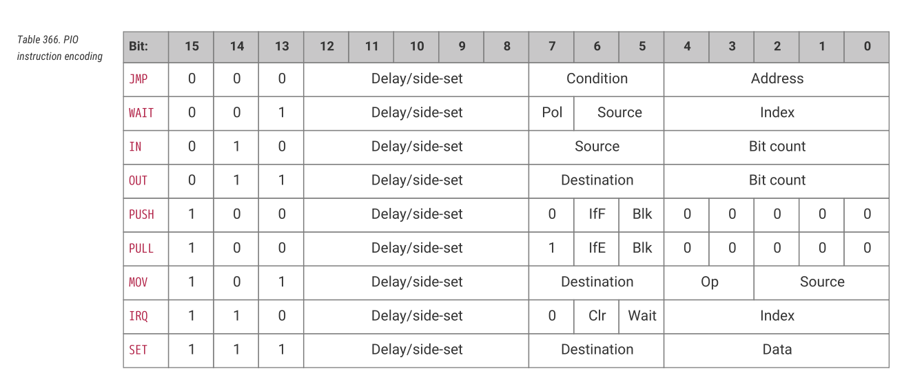
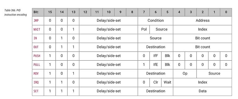
Tabelle der PIO Befehlskodierung
Table 366. PIO instruction encoding Bit: 15 14 13 12 11 10 9 8 7 6 5 4 3 2 1 0 JMP 0 0 0 Delay/side-set Condition Address WAIT 0 0 1 Delay/side-set Pol Source Index IN 0 1 0 Delay/side-set Destination Bit count OUT 0 1 1 Delay/side-set Destination Bit count PUSH 1 0 0 Delay/side-set 0 IfF Blk 0 0 0 PULL 1 0 0 Delay/side-set 1 IfE Blk 0 0 0 MOV 1 0 1 Delay/side-set Destination Op Source IRQ 1 1 0 Delay/side-set 0 Clr Wait Index SET 1 1 1 Delay/side-set Destination Data
in „PiPico PIO programmieren“ · Mikrocontroller und Digitale Elektronik · · Screenshots
-
 Bild
Bild
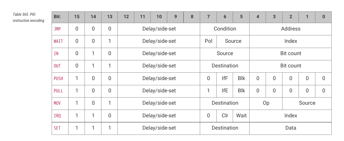
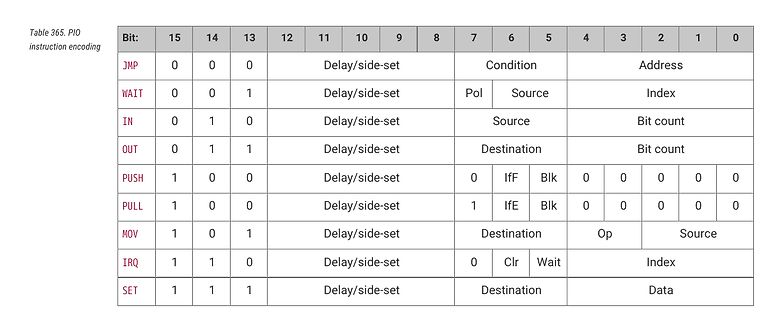
Tabelle der PIO Instruction Encoding Bitbelegung
Table 365. PIO instruction encoding Bit: 15 14 13 12 11 10 9 8 7 6 5 4 3 2 1 0 JMP 0 0 0 Delay/side-set Condition Address WAIT 0 0 1 Delay/side-set Pol Source Index IN 0 1 0 Delay/side-set Source Bit count OUT 0 1 1 Delay/side-set Destination Bit count PUSH 1 0 0 Delay/side-set 0 IfF Blk 0 0 0 PULL 1 0 0 Delay/side-set 1 IfE Blk 0 0 0 MOV 1 0 1 Delay/side-set Destination Op Source IRQ 1 1 0 Delay/side-set 0 Clr Wait Index SET 1 1 1 Delay/side-set Destination Data
in „Datenblatt vom Raspberry Pi“ · Mikrocontroller und Digitale Elektronik · · Screenshots
-
Datei
PPyElektronicCalculator_RevB3_09Feb2014.py
# Rahmen für Dateiwahl und Ende Rahmen1 = Frame(Mainwindow, background = "#002040") Rahmen1.pack(side = TOP, fill = X) #Rahmen2 Rahmen2 = Frame(Mainwindow, background = "#002040") Rahmen2.pack(side = TOP, fill = X) #Rahmen3 Rahmen3 = Frame (Mainwindow, background = "#002040") Rahmen3.pack(side = TOP, fill = X) #Rahmen4 Rahmen4 = Frame (Mainwindow, background = "#002040") Rahmen4.pack(side = TOP, fill = X) #Rahmen5 Rahmen5 = Frame (Mainwindow, background = "#002040") Rahmen5.pack(side = TOP, fill = X) #Rahmen6 Rahmen6 = Frame (Mainwindow, background = "#002040") Rahmen6.pack(side = TOP
in „Layout Programme“ · Platinen ·
-
PDF
semi_eng_ge2a_aqw21_e.pdf
Indicate the peak AC and DC values. *2.Tape and reel packing style X: picked from the 1/2/3/4-pin side. For part numbers with picked from the 5/6/7/8-pin side, change the "X" at the end to "Z" when ordering. Panasonic Industry Co., Ltd. Electromechanical Control Business Division industrial.panasonic.com
in „China-PC817 Optokoppler PCBs“ · Analoge Elektronik und Schaltungstechnik ·
-
PDF
slva963.pdf
running at 8-A continuous output, and left for a period of time to come to thermal equilibrium. The top-side plot was recorded from above while the bottom was recorded from below, looking up. Figure 16. Layout 1 - Single Sided, All Components Top Side Figure 17. Layout 2 – Double Sided, Inductor Top Side, IC Bottom Side Figure 18. Layout 3 – Double Sided, Inductor Top Side, IC Bottom Side 8 Reduced Size, Double-Sided Layout for High-Current DC/DC Converters SLVA963–April 2018 Submit Documentation Feedback Copyright
in „Überlappende Bauteile auf Top und Bottom Layer“ · Platinen ·
-
PDF
auirs2123.pdf
operational sections of this specification is not implied Symbol Definition Min. Max. Units V BS High Side Floating Supply Voltage -0.3 25 V VB High Side Driver Output Stage Voltage -0.3 625 V VS High Side Floating Supply Offset Voltage V B- 25 VB+ 0.3 V V HO Output Voltage Gate Connection VS– 0.3 V B 0.3
in „High-Side Treiber Baustein“ · Analoge Elektronik und Schaltungstechnik ·
-
PDF
doc4834.pdf
used 11 n. u. Not used 12 n. u. Not used Short circuit detected: set high when at least one high-side or low-side 13 SCD switch is switched off by a short-circuit condition. Bits 1 to 6 can be used to detect the shorted switch. Open load detected: set high, when at least one active high-side or 14 OPL
in „DCC Decoder“ · Projekte & Code ·
-
PDF
PSS15NC1FT.pdf
● For N-side : Drive circuit, Control supply under-voltage protection (UV), Short circuit protection (SC) by detecting voltage of external shunt resistor ● Fault signaling : Corresponding to SC fault (N-side IGBT
in „ein echter Monsterchip“ · Offtopic ·
-
PDF
Linear_Current_Sense_AN105.pdf
accurate. The finite current gain of the bipolar tran- sistor isa sourceof small gainerror. High Side-1 APPLICATION NOTE 105: Current Sense Circuit Collection Self-Powered High Side Current Sense Precision High Side Power Supply Current Sense 1.5mΩ VREGULATOR 2 – 8 7 OUT LTC6800 OF LOAD 3 + 6 10k CURRENT
in „'High Side' Strom Messen - Geht das so ?“ · Analoge Elektronik und Schaltungstechnik ·
-
PDF
AN105.pdf
accurate. The finite current gain of the bipolar tran- sistor isa sourceof small gainerror. High Side-1 APPLICATION NOTE 105: Current Sense Circuit Collection Self-Powered High Side Current Sense Precision High Side Power Supply Current Sense 1.5mΩ VREGULATOR 2 – 8 7 OUT LTC6800 OF LOAD 3 + 6 10k CURRENT
in „High-Side Strommessung AVR (Shunt)“ · Mikrocontroller und Digitale Elektronik ·
-
PDF
AD815_SOP.pdf
Output Step Size Figure 25. Open-Loop Transresistance vs. Temperature –85 15 V = ⴞ15V VS= ⴞ15V S SIDE B RL= 150⍀ –80 +PSRR 14 +V SIDE A t OUT o V | –V | B–75 –13 OUT d I – W +V R S OUT S T R L 25⍀ P–70 P12 SIDE A U O | –OUT | –65 SIDE B 11 –PSRR –60 10 –40 –20 0 20 40 60 80 100 –40 –20 0 20 40 60 80
-
PDF
RPS-500-spec.pdf
fan on the top) Case No. 269A-D 247D-T Unit:mm 126 5.0 120 2 5 2 2 3 4 7 3 L4 R M3 5 1.75 2 5 15.5 Side View Side View Side View Top View Air flow direction Side View 130 5 2 8 M3 L= 3 4- 120 8 6 0 1 1 1 Bottom View 1 File Name:RPS-500-SPEC 2020-10-20 500W 5"×3" Reliable Green Medical Power Supply RPS-500 series RPS-500-SF (Enclosed type with fan on the side) Case No. 248B Unit:mm 160 4 3 Side View Air flow 6 direction Side View Side View Top View Side View 130 4M 5.0 3L= 2 1 1 0 5 120 6 Bottom View File Name:RPS-500-SPEC 2020-10-20 500W 5"×3" Reliable
in „Trafo für PCB gesucht.“ · Analoge Elektronik und Schaltungstechnik ·
-
PDF
51292S.pdf
AC244028 Dimensions are in inches 14-Pin Target Pin 1 Located 20-Pin Target Pin 1 Located on Bottom side of Header on Bottom side of Header 28-Pin Target Pin 1 Located 6 Conductor Single In-line on Bottom side of Header Debugger Interface 1.945 1.400 0.855 0.280 1.860 2.370 Optional SPI trace Top 2-Pin
in „PIC18F877 ICD2 bzw Brenner gesucht :-(“ · Mikrocontroller und Digitale Elektronik ·
-
PDF
MP6528.pdf
phase A. Connect a ceramic capacitor to SHA. 5 BSTA See Applications Information section. 6 SHA High-side source connection phase A. 7 GHA High-side gate drive phase A. 8 GLA Low-side gate drive phase A. 9, 10, NC No connection. Leave these pins open. 11, 12 13 BSTB Bootstrap phase B. Connect a ceramic capacitor to SHB. See Applications Information section. 14 SHB High-side source connection phase B. 15 GHB High-side gate drive phase B. 16 GLB Low-side gate drive phase B. 17 LSS Low-side source connection. 18 PWMB PWM input pin for phase B. High drives phase B high; low
in „H-Brücke 48V, PWM 50kHz, Möglichkeit 100% Duty Cycle on“ · Analoge Elektronik und Schaltungstechnik ·
-
PDF
ADuM5400.pdf
As the secondary side DATA DATA converter begins to accept power from the primary, the V I/O I/O ISO 4-CHANNEL 4-CHANNEL voltage startstorise.When the secondaryside UVLOisreached, 0 the secondary side outputs are initialized
in „ADUM5400 (Optokoppler) läuft nicht korrekt“ · Mikrocontroller und Digitale Elektronik ·
-
PDF
BTS7960_v1.1_2004-12-07.pdf
side V OUT = 0 V T j< 85 °C – – 50 µA V INH= 0 V V OUT = 0 V T j= 150 °C 4.2.3 Reverse diode V DS(HS) V IOUT = -9 A forward-voltage high – 0.9 1.5 T j= -40 °C side 1) – 0.8 1.1 T = 25 °C j – 0.6 0.8 T j= 150 °C Low Side Switch - Static Characteristics 4.2.4 On state low side R ON(LS) mΩ IOUT = -9 A resistance V S= 13.5V – 9 12 T = 25 °C j – 14 18 T j= 150 °C 4.2.5 Leakage current low IL(LKLS) – – 1 µA V INH= 0 V side
in „H-Brücke für Gleichstrommotor 24V 5A“ · Analoge Elektronik und Schaltungstechnik ·
-
PDF
Infineon-BTS7960-DS-v01_01-en.pdf
side V OUT = 0 V T j< 85 °C – – 50 µA V INH= 0 V V OUT = 0 V T j= 150 °C 4.2.3 Reverse diode V DS(HS) V IOUT = -9 A forward-voltage high – 0.9 1.5 T j= -40 °C side 1) – 0.8 1.1 T = 25 °C j – 0.6 0.8 T j= 150 °C Low Side Switch - Static Characteristics 4.2.4 On state low side R ON(LS) mΩ IOUT = -9 A resistance V S= 13.5V – 9 12 T = 25 °C j – 14 18 T j= 150 °C 4.2.5 Leakage current low IL(LKLS) – – 1 µA V INH= 0 V side
in „BTS7960 IS Sensor mit abweichenden Werten.“ · Analoge Elektronik und Schaltungstechnik ·
-
PDF
BTS7960_v1.1_2004-12-07.pdf
side V OUT = 0 V T j< 85 °C – – 50 µA V INH= 0 V V OUT = 0 V T j= 150 °C 4.2.3 Reverse diode V DS(HS) V IOUT = -9 A forward-voltage high – 0.9 1.5 T j= -40 °C side 1) – 0.8 1.1 T = 25 °C j – 0.6 0.8 T j= 150 °C Low Side Switch - Static Characteristics 4.2.4 On state low side R ON(LS) mΩ IOUT = -9 A resistance V S= 13.5V – 9 12 T = 25 °C j – 14 18 T j= 150 °C 4.2.5 Leakage current low IL(LKLS) – – 1 µA V INH= 0 V side
in „H-Brücken IC schalten bei Belastung ab und nicht wieder an“ · Mikrocontroller und Digitale Elektronik ·