-
PDF
IMOR100E-01E_010.pdf
power switch is turned OFF. 2 Attach the clamp filter that came with theAC adapter to the output side of the cable of the AC adapter (see figure below). DC output side (Connects to the OR100E/OR300E) 2 B Approx. 10 cm f Clamp filter A1193MN r O p r t o n AC input side (Connects to the power plug) 3
in „Yokogawa OR100E/OR122 wofür?“ · Mechanik, Gehäuse, Werkzeug ·
-
PDF
6N136.pdf
3. Standard dual-in-line package 4. Recognized by UL, file No. E64380 1 1 2 3 4 2 3 4 0.8 Primary side mark ± 0.3 Applications Sunken place) 7.62 ± 0.5 1. Computers, measuring instruments, control P . 9.22 equipment 5 ± 0 . 2. High speed line receivers, high speed logic 3 0 3. Telephone sets ± θ = 0
in „Optokoppler verschleiert Flanken“ · Mikrocontroller und Digitale Elektronik ·
-
PDF
pc847x_SHA.pdf
hola~avoltageshallbemea8uredhthe6RowlIlgmethod. (11 Short between ancde ta cathode an the primary side and between coUfxtor &I emiti on the secondary side. 8.2 Colkctorcurrfmac] DeIweryranktabk ro’lrnflzk~tes~ dcaungPaXLlCofOrdmdpKuduct) Rankat BU&lUs Rankat l Buafnese lc(mAl Test ddtvczy deatfng- -
in „Displaybeleuchtung mit PWM dimmen“ · Mikrocontroller und Digitale Elektronik ·
-
PDF
LPC2129EB_REVB.pdf
info@heissel.de Rev. B, 11/2004 6 LPC2129 Evaluation Board LPC2129 EB 7. Board Layout Fig 4. Top Side Fig 5. Bottom Side Copyright © 2004, Ingenieurbuero Heissel Phone: +49 7557-820767, Fax: +49 7557-820765 Subject to change without notice info@heissel.de Rev. B, 11/2004 7 LPC2129 Evaluation Board LPC2129
in „Einsteigerboard LPC2119(29/94)“ · Mikrocontroller und Digitale Elektronik ·
-
Datei
main.c
constants #define FCPU 16000000 /* CPU speed */ #define GreenLed 7 /* the pin number of the green side of the bi coloured led*/ #define RedLed 6 /* the pin number of the red side of the bi coloured led*/ #define keypin 3 static uint16_t voltage_100,voltage_300,pwm_100,pwm_300; static uint16_t setpnt
in „C-Programm compilieren“ · Mikrocontroller und Digitale Elektronik ·
-
PDF
SD_Multiplexing-Schaltung_im_CPLD.PDF
example, if the host wants to send data to the SD1 device, the host would begin by driving the A side Low. Upon driving Low, the logic in the circuit detects the Low going edge and responds by enabling the ’B’ output buffer, but continues to keep the ’A’ output buffer disabled. Specifically, when A
in „Bidirektionaler Multiplexer im CPLD“ · FPGA, VHDL & Co. ·
-
Datei
main.c
define DIR LATAbits.LATA9 // PIN 28 RA9 // DIR PIN DRIVER //Communikation Ports // PIN 52 U1 RX (UC Side) Pin 53 U1 TX (UC SIDE) // Serial Port 1 "ZIGBEE" // Seriel Port 2 "MP3 PLAYER" // Interface Ports #define ON_OFF LATBbits.LATB7 //RB7 PIN27 // ON/ OFF Button #define SETUP LATBbits.LATB12 // RB12 PIN
in „PIC32 sendet nur 0x00 über UART (MPLABX)“ · Mikrocontroller und Digitale Elektronik ·
-
PDF
X32_on_Trenz_TE300_board.pdf
The main complexity of this module is due to the di▯erent clocks. The SDRAM interface works on one side with the falling edge of a 100MHz clock for the commands and the address path. On the other side the data path works with the rising edge of the same clock shifted 90 degrees. Thus, some additional
in „X32 Softcore“ · FPGA, VHDL & Co. ·
-
PDF
LTV8X4-DB.pdf
shall be measured using the following method. (1) Short between anode and cathode on the primary side and between collector and emitter on the secondary side. (2) The isolation voltage tester with zero-cross circuit shall be used. (3) The waveform of applied voltage shall be a sine wave. *2. For 10
in „Optokoppler LTV824“ · Mikrocontroller und Digitale Elektronik ·
-
PDF
dip203-6.pdf
SSD1803 (SEHR ÄHNLICH ZU HD44780) * ANSCHLUSS AN 4- ODER 8-BIT DATENBUS * SERIELLES SPI-INTERFACE (SID, SOD, SCLK, CS) * SPANNUNGSVERSORGUNG +3,3 V / typ. 4 mA (O. BELEUCHTUNG) * BETRIEBSTEMPERATURBEREICH -20..+70°C * AUTOMATISCHE TEMPERATURKOMPENSATION * LED-BELEUCHTUNG WEISS, max. 75mA@+25°C * 16 ICONS
in „DIP203 LCD mit TMS320F28335 per SPI“ · Mikrocontroller und Digitale Elektronik ·
-
PDF
Linear_Power_MOSFETS_Basic_and_Applications.pdf
current and is bounded by a positive slope line defined by the R ds (on) the device. The right hand side of each line is terminated at the rated drain-to-source voltage limit (Vdss). Each line has a negative slope and is determined by the maximum allowed power dissipation of the device Pd: Pd= [T J (max
in „Gleichstromlast MOSFET“ · Analoge Elektronik und Schaltungstechnik ·
-
PDF
hmo3524-datasheeten.pdf
HO3508 Persistence: Off, 50 ms...∞ 0...2 Million x (1/samplerate) Auxiliary input: Frontside [Rear side] Delay pretrigger: Function Ext. Trigger posttrigger: 0...8 Million x (1/samplerate) Impedance 1 MΩ || 13 pF ±2 pF Display refresh rate: Up to 2500 waveforms/s Coupling DC, AC Display: Dots, vectors
in „Hameg HMO3524“ · Markt ·
-
PDF
CD4009-10_TI.pdf
, protrusions, or gate burrs. Mold flash, protrusions, or gate burrs shall not exceed 0.15 mm per side. 4. This dimension does not include interlead flash. Interlead flash shall not exceed 0.25 mm per side. 5. Reference JEDEC registration MO-153. www.ti.com EXAMPLE BOARD LAYOUT PW0016A TSSOP - 1.2 mm
in „Dipl. Ing Heinz Ahborn Orgel - Keine Töne mehr“ · Analoge Elektronik und Schaltungstechnik ·
-
PDF
LTV_844.pdf
shall be measured using the following method. (1) Short between anode and cathode on the primary side and between collector and emitter on the secondary side. (2) The isolation voltage tester with zero-cross circuit shall be used. (3) The waveform of applied voltage shall be a sine wave. *2. For 10
in „12V 2A per Raspberry Pi (3,3V) schalten“ · Analoge Elektronik und Schaltungstechnik ·
-
Datei
MKL25Z4.h
_t CLPS; /**< ADC Plus-Side General Calibration Value Register, offset: 0x38 */ __IO uint32_t CLP4; /**< ADC Plus-Side General Calibration Value Register, offset: 0x3C */ __IO uint32_t CLP3; /**< ADC Plus-Side General Calibration Value Register, offset: 0x40 */ __IO uint32_t CLP2; /**< ADC Plus-Side General Calibration Value Register, offset: 0x44 */ __IO uint32_t CLP1; /**< ADC Plus-Side General Calibration Value Register, offset: 0x48 */ __IO uint32_t CLP0; /**< ADC Plus-Side General Calibration
in „Interrupts bei Keil ARM? (KL25Z)“ · Mikrocontroller und Digitale Elektronik ·
-
 Bild
Bild
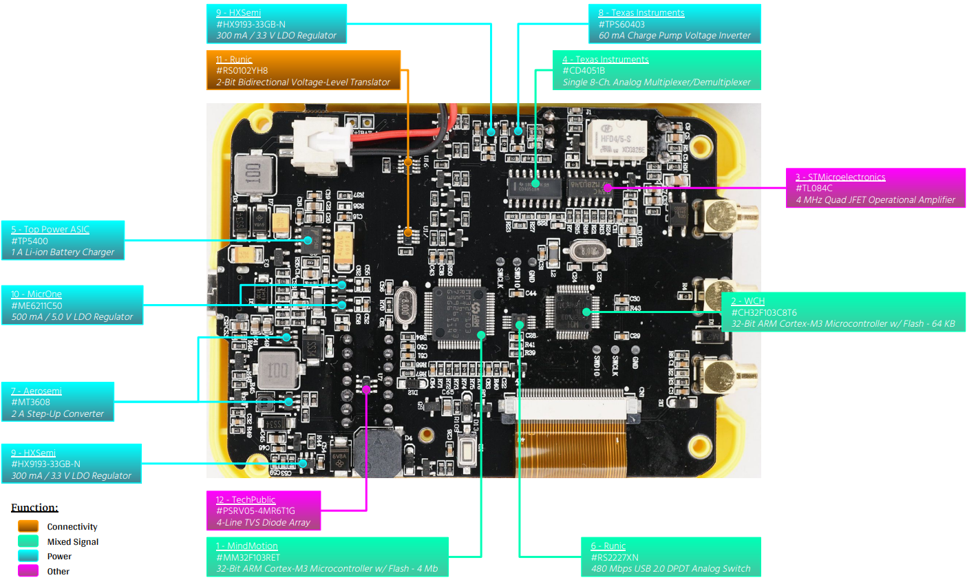
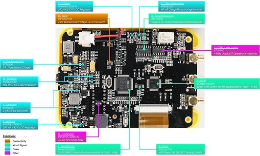
Beschriftete Leiterplatte mit Bauteilbeschreibungen
9 - HXSemi #HX9193-33GB-N 300 mA / 3.3 V LDO Regulator 11 - Runic #RS012YH8 2-Bit Bidirectional Voltage-Level Translator 5 - Top Power ASIC #TPS400 1A Li-ion Battery Charger 10 - MicOne #ME6211C50 500 mA / 5.0 V LDO Regulator 7 - Aerossem #MT3608 2A Step-Up Converter 9 - HXSemi #HX9193-33GB-N 300 mA / 3.3 V LDO Regulator 12 - TechPublic #PSRV05-4MR61TG 4-Line TVS Diode Array 6 - Runic #RS2227XN 480 Mbps USB 2.0 DPDT Analog Switch 1 - MindMotion #MM32F103RET 32-Bit ARM Cortex-M3 Microcontroller w/ Flash - 4 Mb 2 - WCH #CH32F103C8T6 32-Bit ARM Cortex-M3 Microcontroller w/ Flash - 64 KB 3 - STMicroelectronics
in „Transistortester AVR“ · Projekte & Code · · Platinenfotos
-
PDF
Display.pdf
Supply Circuit Pins SYMBOL I/O DESCRIPTION Connecting pin for the internal booster’s capacitor + side. CAP+ O The capacitor is connected between CAP— and CAP+. CAP— O Connecting pin for the internal booster’s capacitor — side. The capacitor is connected between CAP+ and CAP—. Connecting pin for the internal booster’s capacitor + side. VEE2 O The capacitor is connected between V and V EE. Connecting pin for the internal booster’s capacitor + side. VEE3 O The capacitor is connected betweenSS and V EE. Voltage supply pin for generating
in „LC-Display Sharp M078CKA ansteuern“ · Mikrocontroller und Digitale Elektronik ·
-
PDF
lh155.pdf
Supply Circuit Pins SYMBOL I/O DESCRIPTION Connecting pin for the internal booster’s capacitor + side. CAP+ O The capacitor is connected between CAP— and CAP+. CAP— O Connecting pin for the internal booster’s capacitor — side. The capacitor is connected between CAP+ and CAP—. Connecting pin for the internal booster’s capacitor + side. VEE2 O The capacitor is connected between V and V EE. Connecting pin for the internal booster’s capacitor + side. VEE3 O The capacitor is connected betweenSS and V EE. Voltage supply pin for generating
in „Suche sehr dünnes Grafikdisplay“ · Mikrocontroller und Digitale Elektronik ·
-
PDF
MBM29LV800.pdf
sector unprotection via the RESET pin PACKAGE 48-pin Plastic TSOP (I) 48-pin Plastic TSOP (I) Marking Side Marking Side (FPT-48P-M19) (FPT-48P-M20) 44-pin Plastic SOP 48-pin Plastic FBGA Marking Side (FPT-44P-M16) (BGA-48P-M02) (BGA-48P-M12) 2 MBM29LV800TA -70/-90/-12 /MBM29LV800BA -70/-90/-12 GENERAL DESCRIPTION
in „650Stk. Flashbausteine 29LV800 1Mx8 / 512k x16, 3,3V“ · Markt ·
-
PDF
lh155.pdf
Supply Circuit Pins SYMBOL I/O DESCRIPTION Connecting pin for the internal booster’s capacitor + side. CAP+ O The capacitor is connected between CAP— and CAP+. CAP— O Connecting pin for the internal booster’s capacitor — side. The capacitor is connected between CAP+ and CAP—. Connecting pin for the internal booster’s capacitor + side. VEE2 O The capacitor is connected between V and V EE. Connecting pin for the internal booster’s capacitor + side. VEE3 O The capacitor is connected betweenSS and V EE. Voltage supply pin for generating
-
PDF
KS0073.pdf
selection input. When RS/CS = "Low", selected. When RS/CS = "High", not sel ected.(Low access enable) RW/SID (48) I Read, write In bus mode, used as read/write MPU /Serial input data selection input. When RW/SID = "High", read operation When RW/SID = "Low", write operation. In serial mode, used for data input
in „Eigene Zeichen bei LCD mit KS0073 für blöde“ · Mikrocontroller und Digitale Elektronik ·
-
PDF
ssd1803_2_0.pdf
selected. When RS/CS =”Low”, selected. When in bus mode, used as read/write select. Read/Write / When RW/SID=”high”, read operation. RW/SID I Serial Input - When RW/SID=”Low”, write operation. Data When in serial mode, used as serial data input pin. When in bus mode, used as read/write enable E/SCLK I RW Enable
in „DIP203 LCD mit TMS320F28335 per SPI“ · Mikrocontroller und Digitale Elektronik ·
-
PDF
High_Voltage_Low_Noise_DC_DC_Converters_an118fa.pdf
, the Probe isthusgeneratedduringswitchingtransientswhenpower response is greatest just to either side of the conductor transistors are turned on or off. at the address noted in the title of this appendix. Carsten Associates an118fa AN118-31 Application Note 118 ©1997, Bruce Carsten Associates, Inc.
in „Morpheus + Rudi“ · Mikrocontroller und Digitale Elektronik ·
-
PDF
Infineon-TLE4986C-XTS-M47-DS-v01_10-EN.pdf
of the TLE4986C, the field at the sensor position is positive, as shown in Figure 2. TLE4986 Front side ( branded) 1 2 3 Vs Gnd V OUT S N B Hallprobe Front side Figure 2 Definition of the Positive Magnetic Field Direction 2.3 Functional Description The basic operation of the TLE4986C is to map a „large
in „Hat schon jemand einen TLE4986C programmiert?“ · Mikrocontroller und Digitale Elektronik ·
-
PDF
970DE3U3S3.pdf
permanent damage of the motherboard! FDD connector (33-pin FLOPPY1) (see p.12 No. 27) the red-striped side to Pin1 Note: Make sure the red-striped side of the cable is plugged into Pin1 side of the connector. Primary IDE connector (Black) (39-pin IDE1, see p.12 No. 36) connect the blue end connect the black
-
PDF
rxv396.pdf
Remove 2 screws (6) fixing the Main Unit in Fig. 3. f. While pull out the Main Unit to the Front Panel side, place the Main Unit on its side as shown in Fig. 4. Heat Sink g. Connect to ground by shorting between G201 on P.C.B. MAIN (1) P.C.B. MAIN (1) and the chassis. Note) When unconnected to ground, the
in „Yamaha RX-V396 RDS Fehlersuche“ · Mikrocontroller und Digitale Elektronik ·
-
PDF
Audio_Hilbert_WAR19.pdf
channels, causing the stereo modulator in terms of the input and the carrier image to shift from side to side. frequency ω c. Because the system is not linear and time-invariant, it does not have a frequency response T ( ) Y ( )H ω ( ) Y ( )H ( ) (10a) R 0 RR 1 LR per se. However, allowing the input
in „Breitband-NF-Phasenschieber, DSP mit AVR“ · Digitale Signalverarbeitung / DSP / Machine Learning ·
-
PDF
Using_the_Siemens_S65_Display.pdf
simple the data again and again. The display memory is organized according the picture on the right side. The total number of bytes is 132x176x2, that means in total 0xB580 pixel. The memory is written first in X - direction and second in Y - direction. The parameter OR defines the display orientation.
in „The Siemens S65 132x176, 65536 color display with AVR“ · Projekte & Code ·
-
PDF
Using_the_Siemens_S65.pdf
simple the data again and again. The display memory is organized according the picture on the right side. The total number of bytes is 132 x 176 x 2, that means in total 0xB580 pixel. The memory is written first in X - direction and second in Y - direction. The parameter OR defines the display orientation
in „The Siemens S65 132x176, 65536 color display with AVR“ · Projekte & Code ·
-
Datei
main_martin.c
DIL components, except of the MMC/SD card connector. * * The connector is soldered to the bottom side of the board. It has a simple * eject button which, when a card is inserted, needs some space beyond the connector * itself. As an additional feature the connector has two electrical switches * to detect
-
PDF
TDA1552Q.pdf
power package; 13 leads (lead length 12 mm) SOT141-6 non-concave D x h D E h view B: mounting base side d A 2 B j E A L3 L Q c 1 13 Z e1 w M m e2 v M b p e 0 5 10 mm scale DIMENSIONS (mm are the original dimensions) (1) (1) (1) UNIT A A2 b p c D d Dh E e e1 e 2 Eh j L L3 m Q v w x Z mm 17.0 4.6 0.75 0.48
in „Audioverstärkung“ · Analoge Elektronik und Schaltungstechnik ·
-
PDF
74ac541.pdf
clock drivers and bus oriented transmitter/receivers.TATE outputs a ■ Inputs and outputs opposite side of package, alBowing These devices are similar in function to the 74AC2easier interface to microprocessors u 74ACTC244 while providing flow-through architect■ Output source/sink 24 mA f (inputs on opposite side from outputs). This pin■ 74AC541 is a non-inverting option of the 74AC540 ment makes these devices especially useful as an output L port for microprocessors, allowing ease of layou■ 74ACT541 has TTL-compatible
in „ISP(Tutorial) mit HCT541“ · Mikrocontroller und Digitale Elektronik ·
-
PDF
Cyberpen_Operators_Guide.pdf
scanned. 2. Depress and hold the scan button. 3. Place the scanner tip in the white space on either side of the bar code. 4. With the button still depressed, move the scanner quickly and smoothly over the bar code from start to finish, ending in the white space on the other side of the bar code. The motion
in „Kugelschreiber mit Barcodescanner bei Pollin“ · Mikrocontroller und Digitale Elektronik ·
-
PDF
ASMC-QxB2-Txxxx.pdf
1. Exterior automotive LEDs make them uniquely suitable for use in harsh condi- - Turn signals - Side repeaters tions such as in automotive applications, and in electron- - CHSML ics signs and signals. - Rear combination lamp To facilitate easy pick and place assembly, the LEDs are packed in EIA-compliant tape and reel. Every reel is - Side markers shipped in single intensity and color bin (except for red), - Truck clearance lamp to provide close uniformity. These LEDs are compatible 2. Electronic signs and signals with the IR solder reflow
in „[V] 0,5W LEDs ROT“ · Markt ·
-
PDF
ES150.pdf
with earth loops and common mode voltages. Pin compatible with the programming connector on the rear side. Bench operation and rail mounting. Internal Ethernet Power Supply Controller OPTION P150 Internal Ethernet compatible interface to program a unit by a computer. Combination possible with P119 - P122
-
PDF
LR8.pdf
Package Outline (K4) b3 A E E1 c2 4 L3 θ1 D1 H D 1 2 3 L4 L5 Note 1 b2 View B e b Front View Rear View Side View Gauge Plane A1 Seating L2 Plane θ L L1 View B Note: 1. Although 4 terminal locations are shown, only 3 are functional. Lead number 2 was removed. Symbol A A1 b b2 b3 c2 D D1 E E1 e H L L1 L2 L3
in „20 V AC bis 70 V AC --> 5 V DC“ · Analoge Elektronik und Schaltungstechnik ·
-
PDF
Susumu_rp-rph.pdf
RL3264L4 L (Inch Size) (1206) (2010) (2512) T L 3.2 0.2 5.0 0.2 6.4 0.2 W 1.6 0.2 2.5 0.2 3.2 0.2 Top side W T 0.5 0.15 0.5 0.15 0.5 0.15 a 1.0 0.2 1.7 0.2 2.1 0.2 b 0.55 0.2 0.9 0.2 1.2 0.2 unit : mm a Equivalent circuit b back side V V I I V=Voltage Terminal Electrical I =Current Terminal Type RL1632L4
in „SMD Gehäuseformen“ · Platinen ·
-
PDF
Using_the_Siemens_S65_Display.pdf
simple the data again and again. The display memory is organized according the picture on the right side. The total number of bytes is 132x176x2, that means in total 0xB580 pixel. The memory is written first in X - direction and second in Y - direction. The parameter OR defines the display orientation.
in „Bausatz Add-on für AVR-NET-IO“ · Mikrocontroller und Digitale Elektronik ·
-
PDF
CrumbX128A1_V1.0_infosheet.pdf
it is possible to automatically reset the module in the moment the virtual COM port on the host PC side is being opened by the bootloader PC application or by a terminal program. This is possible by closing jumper J7, which connects the CP2102's DTR signal through a capactor to the MCU's reset signal.
in „[V] LCD Display, xMega128 mit USB, AM/FM Radio Empfänger“ · Markt ·
-
PDF
Tremba_Magnetsteuerung.pdf
Analogeingang Versorgungsspannung PC1 Intern ADC1 Spannungs-Messung: Analogeingang Gate-Spannung High-Side FET PC2 ADC2 Spannungs-Messung: Analogeingang Intern Gate-Spannung Low-Side FET PC3 R19 ADC3 Spannungsmessung: Poti (frei Analogeingang verwendbar) PC4 Kommport Link1 frei verwendbar, alternativ SDA
in „Analosignal mit Microkontroller auslesen“ · Mikrocontroller und Digitale Elektronik ·
-
PDF
Tremba_Magnetsteuerung.pdf
Analogeingang Versorgungsspannung PC1 Intern ADC1 Spannungs-Messung: Analogeingang Gate-Spannung High-Side FET PC2 ADC2 Spannungs-Messung: Analogeingang Intern Gate-Spannung Low-Side FET PC3 R19 ADC3 Spannungsmessung: Poti (frei Analogeingang verwendbar) PC4 Kommport Link1 frei verwendbar, alternativ SDA
in „Spannungsregelung mit MC MST 1630 von Tremba“ · Mikrocontroller und Digitale Elektronik ·
-
PDF
cic1.pdf
sample and previous output sample.] y(n) – y(n-1) = x(n) Eqn (2). Or, Taking z transforms on both sides (where the definition of the z transform is: X(z) = Σ x(n)z . Where the summation is k = -∞ to ∞. ) The variable z is complex. Thus if the z transform is taken on both sides of Eqn (2) we get: -1 Y
in „Verständnis von CIC Decimation“ · Digitale Signalverarbeitung / DSP / Machine Learning ·
-
PDF
AQV21xS.pdf
style voltage current Tube packing style Picked from the Picked from the Tube Tape and reel 1/2/3-pin side 4/5/6-pin side 60V 500mA AQV212S AQV212SX AQV212SZ 100V 300mA AQV215S AQV215SX AQV215SZ 1 tube contains: AC/DC 200V 160mA AQV217S AQV217SX AQV217SZ 75 pcs. dual use 350V 120mA SOP6-pin AQV210S AQV210SX
in „Dualer Optokoppler als Schalter (Auslöser für Kamera) HCPL 0531“ · Mikrocontroller und Digitale Elektronik ·
-
PDF
AN52_-_Small_PCB_Antennas_for_Micrel_RF_Products.pdf
Impedance example of its frequency response for the 433.92 MHz matching. The attenuation on the left side of the graphics To bring its impedance close to 50 ohms or any other is more abrupt in comparison to the right side. This is a impedance value, a shunt inductor from the feeding point nice feature to
in „Small Antenna Design bei 433 MHz“ · Mikrocontroller und Digitale Elektronik ·
-
PDF
AN41204.pdf
Input/Output gain ACS RCS=0.22Ω 1.07 1.33 1.59 A/V Input bias current IBH -1 ⎯ 1 µA <Output> Upper-side output-ON resistance ROH O =−500mA ⎯ 0.32 0.50 Ω Lower-side output-ON resistance ROH IO= 500mA ⎯ 0.29 0.45 Ω Torque limit current ITL RCS0.22Ω 800 1000 1200 mA Electrical Characteristics V DD=VMSP=VMAC
in „DVD-Laufwerk DVS-7150V reparieren“ · PC Hard- und Software ·
-
PDF
GER_CD_2141577_B1_pdf_2141577_c_drw.pdf
Pins. .2 DELIVERY STATUS Layout ist entsprechend auszulegen. ) 2:1 PIN LAYOUT SHOWN FROM SOLDERING SIDE OF PCB. (0.4) DIMENSIONS AND TOLERANCES ACCORDING TO PINS. 7.6) LAYOUT HAS TO BE ADAPTED. 1.8) ▯n▯1.8 mm Bohrung fuer Boardlocks 7 ▯n▯1.8 MM HOLE FOR BOARDLOCKS (3) 24.75 0.3 25.65 ) 8 Steckersystem
in „Bitte um Hilfe bei Bauteilsuche (MOST-BUS)“ · Mikrocontroller und Digitale Elektronik ·
-
PDF
LND150_C041114.pdf
E1 Gauge 0.25 Plane 1 2 L Seating e L1 Plane b e1 Top View View B View B A A2 A Seating Plane A1 Side View A View A - A Symbol A A1 A2 b D E E1 e e1 L L1 θ MIN 0.89 0.01 0.88 0.30 2.80 2.10 1.20 0.20† 0 O Dimension 0.95 1.90 0.54 (mm) NOM - - 0.95 - 2.90 - 1.30 BSC BSC 0.50 REF - MAX 1.12 0.10 1.02
in „DDR- Mosfet SM104 in Sinusgenerator GF22“ · Analoge Elektronik und Schaltungstechnik ·
-
PDF
LTV-356T.pdf
shall be measured using the following method. (1) Short between anode and cathode on the primary side and between collector and emitter on the secondary side. (2) The isolation voltage tester with zero-cross circuit shall be used. (3) The waveform of applied voltage shall be a sine wave. 2. For 10 Seconds
in „1500V 8A mit MOSFET schalten“ · Analoge Elektronik und Schaltungstechnik ·
-
PDF
SY8105ADC.pdf
Inductor pin. Connect this pin to the switching node of inductor BS 6 Boot-Strap Pin. Supply high side gate driver. Decouple this pin to LX pin with 0.1uF ceramic cap. Absolute Maximum Ratings (No e 1) SupplyInput Voltage --------------------------------------------------------------------------19V--
in „Fragen Stromversorgung / Schaltplan“ · Analoge Elektronik und Schaltungstechnik ·
-
PDF
Infineon_TLE4913_DS_v02_03_EN-3363911.pdf
mT 1Positive magnetic fields are related to the approach of a magnetic south pole to the branded side of package Note: The listed AC/DC and magnetic characteristics are ensured over the operating range of the integrated circuit. Typical characteristics specify mean values expected over the production
in „Schachbrettposition Erkennung“ · Mikrocontroller und Digitale Elektronik ·