speed by several orders of magnitude over conventional phototransistor optocouplers by reducing the base−collector 1. ON = onsemi Logo 2. 500 = Device Number capacitance of the input transistor. The HCPL04XX devices do not 3. V = VDE mark indicates have the base bonded out to a lead for additional noise
Verfügung stehen soll. 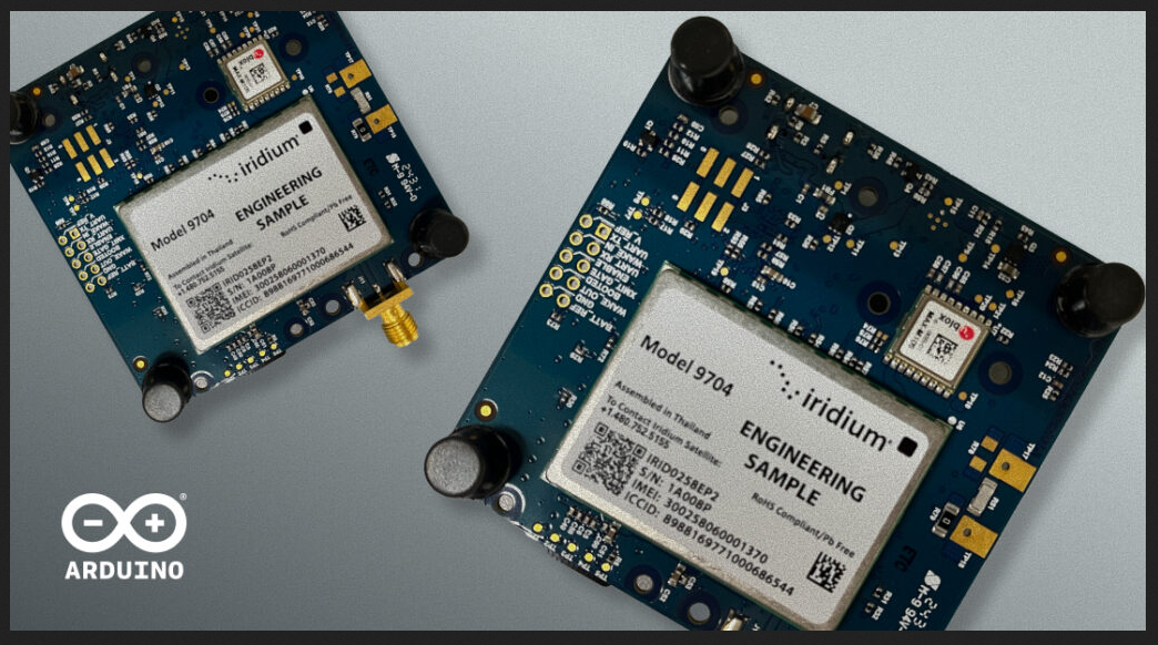 Bildquelle: https://blog.arduino.cc/2025/07/21/dive-into-satellite-iot-with-the-new-arduino-compatible-iridium-certus-9704-development-kit/ Über die Spezifikationen vermeldet man folgendes: [c] To make this as accessible as possible, Iridium
Developer Board was compatible with the Arduino IDE and ecosystem. That board contains a Microchip ATSAMD21J18A microcontroller, which integrates nicely with everything Arduino. The board has UART, SPI, and I2C connections available, as well as 22 digital I/O pins. Of those, 12 are also PWM (pulse-width
Electronics Co.,LTD MX1616H Package Dimensions SOP16ÿ D A3 0.25 A2 A c L A1 ÿ L1 b b1 E1 AND c1 c BASE METAL WITH PLATING b and MILLIMETER SYMBOL MIN NAME MAX - - A 1.77 A1 0.08 0.18 0.28 A2 1.20 1.40 1.60 A3 0.55 0.65 0.75 b 0.39 - 0.48 b1 0.38 0.41 0.43 - c 0.21 0.26 c1 0.19 0.20 0.21 D 9.70 9.90 10.10
MAXIMUM RATINGS (Note 1) Rating Symbol Value Unit Collector−Emitter Voltage V 140 Vdc CEO Collector−Base Voltage VCB 160 Vdc Emitter−Base Voltage VEB 7.0 Vdc Collector Current− Continuous C 10 Adc − Peak 15 TO−204AA (TO−3) CASE 1−07 Base Current − Continuous B 7.0 Adc − Peak − STYLE 1 Total Device Dissipation
to control all I/O registers on the ALL-03 main module. Register name I/O address accesss IDPORT base address+0 Write-only DATAPORT base address+2 read+write The base address is the I/O address of the SAC-201 as defined by DIP switches 1 and 2. These switches allow a choice of 16 possible base addresses
LEAD BENT LEAD BC548 30 TAPE & REEL Collector - Base Voltage VCBO Vdc BC546 80 BC547 50 BC548 30 MARKING DIAGRAM Emitter - Base Voltage VEBO 6.0 Vdc Collector Current − Continuous C 100 mAdc BC 54xy Total Device DissipationA@ T = 25°C P D 625 mW AYWW
OCPP 1.6 JSON Safety Risk assessment Warranty Base warranty 24 months after Site Acceptance Test or 30 months after factory delivery. Warranty extensions available 13 Terra 94 Terra 54 Terra 24 English, Italian, Spanish, German, French, ... and more
provides the input reference clock for the APLL. The on chip internal oscillator provides a time base to support a number of operations, including the detection of the MCLK ratio, the data rate, and clock error conditions. The internal oscillator time base provides a constant rate for all controls and
Ich hab es nicht weiter verfolgt, hängt in der Warteschleife - siehe Issues #21 und #16. Es könnte an meinem Android Chrome Browser liegen, muss das noch mal mit einem anderen Gerät testen. https://github.com/gb88/BLEOTA/issues/21 Ich hab nun erstmal das ElegantOTA Lite verwendet
. [c] ElegantOTA.loop(); [/c] Passwort steht als Klartext im Sketch, könnte man sicher noch base64 maskieren aber ich denke das reicht mir so als Sicherheit. [c] const char* ssid = "ESP32"; const char* password = "12345678"; [/c]
peripheral occupies a certain address space, and the actual access address of peripheral register is: base address + offset address. In the following chapters, the address of the register is described in detail. The following table shows the assignment of base address of each peripheral. Table 2-5 Peripheral base address assignment table Peripheral No. Peripheral name Peripheral base address 1 SYS (PMU/RTC/GPIO/KEY SCAN, etc.) 0x4000 1000 AUX (PLL/CMP, etc.) 2 FlashROM-Control 0x4000 1800 3 TMR 0x4000 2400 4
200µF) 18.2kO PRI 5kO 63.4kO ST OV1 5kO TPS2121 IN2 IN2 (5V) 10.2kO SS 1µF CP2 5kO 23.7kO ILM OV2 21.5kO GND 5kO Figure 10-9. Automatic Switchover Between 12 V and 5 V 10.3.2 Design Requirements Table 10-3. Automatic Switchover Design Requirements DESIGN PARAMETER SPECIFICATION DETAILS IN1 Voltage V
Max schrieb im Beitrag #7883124: > https://usa.shelly.cloud/knowledge-base/shelly-25/ ab 24 VDC > Das scheinen aber nur Schließerkontakte zu sein. 2 Ausgänge 1* Power 1* Richtung über 2*um Relais.
der Shelly via Software schon, und die Motoren sind da üblicherweise resistent gegen, wir sind im 21. Jahrhundert. Ein einfacher Umpolkondensatorrohrmotor kostet nur wenige € weniger als einer mit Blockierschutz und Elektronik drin, und der kann dann auch an beiden Polen gleichzeitig angesteuert werden
Martin A. schrieb im Beitrag #7881612: > JSW79. Was ist das denn für ein Transistor? BAS21 Diode https://assets.nexperia.com/documents/data-sheet/BAS21.pdf
INTERNATIONAL IEC STANDARD 62056-21 First edition 2002-05 Electricity metering – Data exchange for meter reading, tariff and load control – Part 21: Direct local data exchange This English-language version is derived from the original
21. Single-cycle ALU Operation T1 T2 T3 T4 System Clock Ø Total Execution Time Register Operands Fetch ALU Operation Execute Result Write Back The internal data SRAM access is performed in two System Clock
Hier erhalten Sie eine Hier können Sie auf Übersicht an Informati- Wunsch aktivieren, onen zum Akku. 21 DE AT CH • Statistik Benutzer aus demsel- Hier fjnden Sie die An- ben Haushalt über die zahl der Ladezyklen, Ent- Lidl Home App autori- ladezyklen und die Ge- sieren. Sie fjnden hier samtlaufzeit des
Beispiel hier zu finden: https://www.open-std.org/jtc1/sc22/wg14/www/docs/n3193.htm >> The use of base-8 instead of base-10 by integer literals that begin >> with a zero digit is the source of frequent confusion. We propose >> marking the use of such literals as obsolete in order to encourage >> a
introduction of a new >> prefix to explicitly mark literals that are genuinely intended to >> be in base-8. und: >> We propose that a new syntax is added for explicit octal constants, >> with a new prefix 0o or an alternative spelling to mark the beginning >> of a base-8 literal. The old syntax
forum.zerspanungsbude.net [116.202.240.228]) by xxx(Postfix) with ESMTPS for <yyy>; Sun, 27 Apr 2025 21:28:40 +0200 (CEST) [/pre] Das Einzige, was man ihnen heutzutage wohl übel nehmen wird ist, dass sie kein DKIM aufgesetzt haben.
Subject: =?UTF-8?B?V2lsbGtvbW1lbiBhdWYg4oCeWmVyc3BhbnVuZ3NidWRl4oCc?= Das Subject komplett als Base64 könnte Minuspunkte geben, weil das Spammer gerne verwenden, um Wortfilter zu umgehen. Thomas schrieb im Beitrag #7868392: > X-Spam-Flag: NO > UI-InboundReport: notjunk:1 Scheint sie aber nicht
Die Version von ComputerBase scheint's zu tun, auch wenn sie behauptet, meine GeForce GraKa könnte keine 3D-Beschleunigung... Die von verschiedenen Stellen angebotenen Versionen unterscheiden sich in der Größe gerne mal um
diese liefert Broadcom die entsprechenden Mails aus. Der einliefernde Mailserver ist: [pre] Apr 24 21:19:12 uriah postfix/smtpd[22085]: setting up TLS connection from apps-relay.smtp.broadcom.com[192.19.211.195] [/pre] Wenn ich in dem vorhandenen Account (der sinnlos geworden ist, weil ich meinen
Da beim 2716 Pin 21 (Vpp) wohl auf Vcc liegt, würde das einem 2732 entsprechen, bei dem der Code in der oberen Hälfte des Speichers liegt (A11 = '1'). Dafür könnte man beim erzeugten .hex-Code die Speicheradresse mit einem Offset von 0x800 versehen. Alternativ verbindet man Pin 21 nicht, wodurch dann durch den 'pull-down'-Widerstand A11 = '0' wird. Da ich 2708/2716 garnicht mehr auf dem Schirm hatte, hatte ich MIN_ROM_SIZE auf 0x1000 gesetzt. Die aktuellen Versionen sind
eine Multiplikation bzw. Division und die dürften hier recht häufig genutzt werden. - "RV32E" Base integer instruction set (embedded), 32-bit, 16 registers - "C" Standard extension for compressed instructions - "M" = Standard extension for integer multiplication and division - https://en.wikipedia.org
movqi_insn/2 ldd r18,Y+1 ; 236 [c=16 l=4] *movsf/2 ldd r19,Y+2 ldd r20,Y+3 ldd r21,Y+4 [/pre] und liest Y+1 noch nicht mal aus danach... Damit gewinnt man natürlich keinen Blumentopf. Vermutlich https://gcc.gnu.org/PR110093 o.ä.
TCB consists of a base counter and control logic that can be set in one of eight different modes, each mode providing unique functionality. The base counter is clocked by the peripheral clock with optional prescaling. Complete
MMBFJ312LT1 T܆22B i HE=423291 Q4357 1 nnde†2H§en vur5@nuı1@Hı R2v.Num2er¦ 21 e F-1 = cf-oN 1292 sumecı 10 change wT1T¬o21 manuel / 7 Buufuı 1ØBX/158X V4 ~ı T1 r@42ı†@a #1 H2H2n@;12=K± 9 T 2 | C | 2 T E T F T G | H T 1 T J T K T L I M T N T Ä n d e u n g e n v r b |_ 2 I B I c
. Dazu noch ein bisschen Code: [c]int main (void) { ... /* USER CODE BEGIN 2 */ HAL_TIM_Base_Start (&htim2); HAL_TIM_IC_Start_IT (&htim2, TIM_CHANNEL_1); // main channel HAL_TIM_IC_Start (&htim2, TIM_CHANNEL_2); // indirect channel __enable_irq (); /* USER CODE END 2 *
werden. Musste gerade mal auf meine Armbanduhr schauen. Und – wie erwartet – wir befinden uns im 21. Jahrhundert. Nicht nur dass der Schmitt-Trigger sich mittlerweile weitestgehend etabliert hat, auch die Messmethodik hat durchaus Fortschritte erfahren. So kann man — wenn es denn nötig erscheint
periphery modules they belong to - each periphery module (e.g. RCC, GPIOA, GPIOB, USB, …) has its own base address. The addresses of the individual registers are specified as an offset that needs to be added to this base address to obtain the full absolute address of the register. Chapter 7.3.7 specifies
multiply r8 by 4 (since each word is 4 bytes in size) and add it to r7, which contains the array’s base address. At the end of the loop, r8 is compared with 18, which is the number of entries in the array. This variant is actually less efficient, as it needs to keep both the base address and the index
Pins N 8 Pitch e .100 BSC Top to Seating Plane A - - .210 Molded Package Thickness A2 .115 .130 .195 Base to Seating Plane A1 .015 - - Shoulder to Shoulder Width E .290 .310 .325 Molded Package Width E1 .240 .250 .280 Overall Length D .348 .365 .400 Tip to Seating Plane L .115 .130 .150 Lead Thickness c
