zurückgebaut, nachdem man kurz vorher noch die Leistung gesteigert hat. Ich weiss nicht, ob es in den 70ern schon so war, dass beim Bau eines KKW die Kosten für den Rückbau schon bereitliegen mussten. heute ist es so. Gundremmingen hat damals acht Milliarden DM im Bau gekostet, wobei ich nicht weiss
schrieb im Beitrag #7898314: > neuen Konzepten wie dem MSR Neu ? Du meinst den Scheiss, der seit 70 Jahren nicht funktioniert ? Salzschmelzen sind hochaggressive Chemikalien, quasi Schwefelsäure im Rundrumpumpwerk. Gerhard O. schrieb im Beitrag #7898314: > Thorium-Reaktorkonzept Thorium gibt
Operating temperature range -35 °C to +55 °C -35 °C to +55 °C Storage temperature range -40 °C to +70 °C -40 °C to +70 °C Humidity 20-95 % Rh non-condensing 20-95 % Rh non-condensing Mounting Free-standing cabinet Free-standing cabinet Dimensions (H x W x D) 1900 x 565 x 880 mm 1900 x 565 x 880 mm Mass
provides the input reference clock for the APLL. The on chip internal oscillator provides a time base to support a number of operations, including the detection of the MCLK ratio, the data rate, and clock error conditions. The internal oscillator time base provides a constant rate for all controls and
. Min. Typ. Max. A 0.45 0.62 0.018 0.025 A3 0.08 0.18 0.003 0.007 b 0.17 0.34 0.007 0.013 D 1.50 1.70 0.059 0.067 E 1.50 1.70 0.059 0.067 E1 1.10 1.30 0.043 0.051 e 0.50 0.020 L1 0.19 0.007 L2 0.10 0.30 0.004 0.012 1. Value in inches are converted from mm and rounded to 4 decimal digits DS4260 - Rev
life and property. • Industrial equipment: Products that can be used in industrial equipment such as base stations, manufacturing equipment, industrial robotics equipment, and measurement equipment, and whose functions do not directly relate to the protection of human life and property. • Medical equipment
peripheral occupies a certain address space, and the actual access address of peripheral register is: base address + offset address. In the following chapters, the address of the register is described in detail. The following table shows the assignment of base address of each peripheral. Table 2-5 Peripheral base address assignment table Peripheral No. Peripheral name Peripheral base address 1 SYS (PMU/RTC/GPIO/KEY SCAN, etc.) 0x4000 1000 AUX (PLL/CMP, etc.) 2 FlashROM-Control 0x4000 1800 3 TMR 0x4000 2400 4
. (2) All voltages are with respect to GND. DISSIPATION RATINGS DERATING FACTOR TA≤ 25°C POWER TA= 70°C POWER TA= 85°C POWER PACKAGE ABOVE T A 25°C RATING RATING RATING TSSOP-8 (PW) 3.9 mW/°C 387 mW 213 mW 155 mW SON-8 (DRB) (1) 25.0 mW/°C 2.50 mW 1.38 mW 1.0 W (1) See TI application note SLMA002 for
SBVS044F –MARCH 2004–REVISED MAY 2012 PACKAGE DISSIPATION RATINGS DERATING FACTOR T ≤ 25°C POWER T = 70°C POWER T = 85°C POWER A A A PACKAGE ABOVE T =A25°C RATING RATING RATING TSSOP-8 (PW) 3.9 mW/°C 387 mW 213 mW 155 mW SON-8 (DRB) 25.0 mW/°C 2.50 W 1.38 W 1.0 W RECOMMENDED OPERATING CONDITIONS MIN NOM
one is Installed installed. 500–BIOS Recovery A system BIOS recovery has occurred. Not applicable. 70x-Wireless Mode Not Supported The system has detected a wireless module Replace with a supported module. installed in the system that is not supported and has been disabled. 800-Keyboard Error Keyboard
der den Übergang weicher macht, wenn die Endtransistoren leitend werden, und beim Abschalten die Basen schneller räumt. Nur R29 und R30 sind der eigentliche Spannungsteiler. Wie siehst Du das?
Meinen dann halt das es der Maschiene egalt ist ob se übern Tag verteilt 10 Tassen raus lässt, oder 70 Tassen am Stück. Und dann nehmen diese Bauteile halt das übel. Meiner Meinung nach, sind die Standardmaschinen nicht für 100% ED ausgelegt, und das bewusst, um Unterschiede auch im Preis abbilden zu
C A 20 A ( 15 O I 10 5 0 0 0.5 1 1.5 2 2.5 3 VOP (V) 80 AT90S2313 0839I–AVR–06/02 AT90S2313 Figure 70. I/O Pin Sink Current vs. Output Voltage I/O PIN SINK CURRENT vs. OUTPUT VOLTAGE Vcc 5V 70 T A 25˚C 60 T = 85˚C A 50 40 ) A ( 30 O I 20 10 0 0 0.5 1 1.5 2 2.5 3 VOL (V) Figure 71. I/O Pin Source Current
batterie Service-Center.........91 à l‘application Importateur.............91 Lidl Home................70 59 FR BE Pièces de rechange/ des instructions impor- Accessoires..............92tantes pour la sécurité, Traduction de la décla- l’utilisation et l’élimina- ration de conformité CE tion des déchets.
volatile unsigned int WKUPEPR; /* PWR wakeup enable and polarity register */ }; #define PWR_BASE 0x58024800 #define PWR ((struct stm32_pwr *) PWR_BASE) [/c] Zugreifen auf die einzelnen Register kannst du dann so: [c] PWR->CR1 = 0x1234ABCD
define ULONG_MAX 4294967295 #define ULLONG_MAX 18446744073709551615 [/code] Quelle: http://port70.net/%7Ensz/c/c11/n1570.pdf [Annex E - Implementation limits] Zu einem LCD-Controller mit 32-Bit Registern hab ich mal ChatGPT befragt und der hat ein paar ausgegeben. War zu Faul um selber zu suchen
to 7.5 A at 80 °C. systems – high packing density and at the same time Based on the plug uniform base centerline of 2.54 mm, high load of current carry- the MQS interconnection ing capacity, robust design ranges from MQS and Micro and safe handling – were consistently implemented. Power Quadlok to Power
Beispiel hier zu finden: https://www.open-std.org/jtc1/sc22/wg14/www/docs/n3193.htm >> The use of base-8 instead of base-10 by integer literals that begin >> with a zero digit is the source of frequent confusion. We propose >> marking the use of such literals as obsolete in order to encourage >> a
introduction of a new >> prefix to explicitly mark literals that are genuinely intended to >> be in base-8. und: >> We propose that a new syntax is added for explicit octal constants, >> with a new prefix 0o or an alternative spelling to mark the beginning >> of a base-8 literal. The old syntax
Da es sich hierbei um ASCII-Dateien handelt, reicht die Ausgabe über ein 'type' wie es im Beispiel 'bas.bat' gezeigt wird. Nach Initialisierung des Programms wird die Routine 'rom_simulation()' ausgeführt, die permanent die Adressleitungen einliest und das zugehörige Datenbyte aus dem 'rom_puffer[]
Ausgang geht. Oder (selbst erlebt) die aktuelle Spur der Floppy wird formatiert (dazu reichte in den 70ern das Schreiben eines einzigen Bytes an die "falsche" Adresse), setzt aber voraus, daß der Floppy-Motor an ist. > In den 70ern waren wohl 74LS14 mit RC-Glied eine typische > Resetschaltung, die
Soldering problems caused by oil in the connectors can be avoided by placing the compressor on its base Connector positions plate some time before soldering it into the system. The compressor must never be placed upside down when mounting the rubber grommets in the base plate. Instead place the compressor
Jetzt sinds für Bestandskunden schon 3.49, zuzüglich Versand, wobei der ab 10 Euro nix kostet. 70 Cent pro Platine ist immer noch lächerlich günstig.
Harald K. schrieb im Beitrag #7973497: > 70 Cent pro Platine ist immer noch lächerlich günstig. Das stimmt! Aber es ist auch nicht nur der Preis. Datenblatt, Software, funktioniert auch in Arduino, das ist alles schon ganz gut. Und du weißt
Architecture 7. Peripherals and Architecture 7.1 Peripheral Address Map The address map shows the base address for each peripheral. For complete register description and summary for each peripheral, refer to the respective sections. Table 7-1. Peripheral Address Map Base Address Name Description 0x0000
127135 I ' 1NF R70e0 w RD-1-12V M 3 6 Z 2 h R7171 R7170 |5 *WEPF W 20 RD+12v 7097 IÜA 22014/F0[1E Rmm W49 7 mm.E2DD1 51'“ 1717D13e40 ,Q E IIII0R70saDRQ u VR70D4 n I5 C017R »v 17 RD»12v RURGV 10K0 RD-1-12V 50K o C7104 c
NTS4409N, NVS4409N MOSFET – Single, N-Channel, Small Signal, ESD Protection, SC-70/SOT-323 25 V, 0.75 A http://onsemi.com Features V(BR)DSS R DS(on)yp IDMax • Advance Planar Technology for Fast Switching, Low R DS(on) 249 mW @ 4.5 V 25 V 0.75 A • Higher Efficiency Extending Battery
. Dazu noch ein bisschen Code: [c]int main (void) { ... /* USER CODE BEGIN 2 */ HAL_TIM_Base_Start (&htim2); HAL_TIM_IC_Start_IT (&htim2, TIM_CHANNEL_1); // main channel HAL_TIM_IC_Start (&htim2, TIM_CHANNEL_2); // indirect channel __enable_irq (); /* USER CODE END 2 *
auch, ca 100€ auf dem Gebraucht Markt. > Ein professioneller Zähler halt. Wenn wir schon in den 70ern+++ sind, wie wäre es mit 2 x 74390, 2 x 74374, 4 x 7447 und etwas wie 7408 und 7414? Vielleicht gibt es diese Teile ja schon in stromsparender Version? ;-)
periphery modules they belong to - each periphery module (e.g. RCC, GPIOA, GPIOB, USB, …) has its own base address. The addresses of the individual registers are specified as an offset that needs to be added to this base address to obtain the full absolute address of the register. Chapter 7.3.7 specifies
multiply r8 by 4 (since each word is 4 bytes in size) and add it to r7, which contains the array’s base address. At the end of the loop, r8 is compared with 18, which is the number of entries in the array. This variant is actually less efficient, as it needs to keep both the base address and the index
applications from 350 nm to 970 nm - Adapted to human eye sensitivity (V ) λ - SMT package without base connection, suitable for IR reflow soldering - Only available on tape and reel - Smart-DIL package - Spectral range of sensitivity: (typ) 350 ... 970 nm 2 | Version 1.6 | 2024-12-06 SFH 3410 DATASHEET
Current vs Temperature 100 20 90 SCL = 100 kHz VCC = 2.5 V All I/Os unloaded 18 ) 80 16 TA= −40ºC A ( 70 ) 14 n A T = 25ºC e 60 ( 12 A u 50 N 10 C I p 40 8 p S 30 6 20 4 TA= 85ºC 10 2 0 0 2.0 2.5 3.0 3.5 4.0 4.5 5.0 5.5 0.0 0.1 0.2 0.3 0.4 0.5 0.6 Supply Voltage (V) Vol (V) Figure 4. I/O Sink Current vs
Pins N 8 Pitch e .100 BSC Top to Seating Plane A - - .210 Molded Package Thickness A2 .115 .130 .195 Base to Seating Plane A1 .015 - - Shoulder to Shoulder Width E .290 .310 .325 Molded Package Width E1 .240 .250 .280 Overall Length D .348 .365 .400 Tip to Seating Plane L .115 .130 .150 Lead Thickness c
material (3) (4/5) (6) LM3886T/NOPB ACTIVE TO-220 NDJ 11 20 RoHS & Green SN Level-1-NA-UNLIM 0 to 70 LM3886T LM3886TF ACTIVE TO-220 NDA 11 20 Non-RoHS & Call TI Call TI 0 to 70 LM3886TF Non-Green LM3886TF/NOPB ACTIVE TO-220 NDA 11 20 RoHS-Exempt SN Level-1-NA-UNLIM 0 to 70 LM3886TF & Non-Green (1The
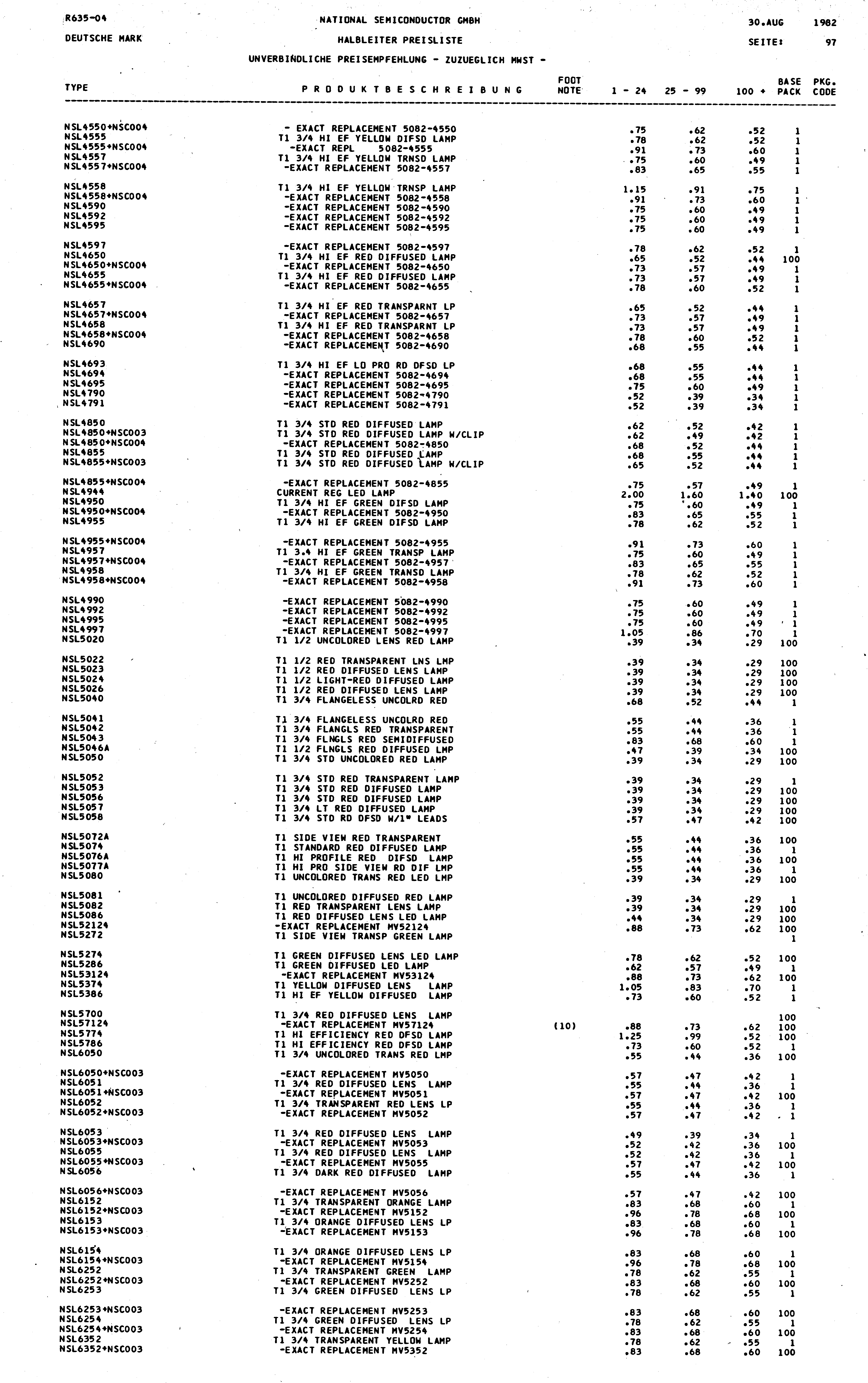
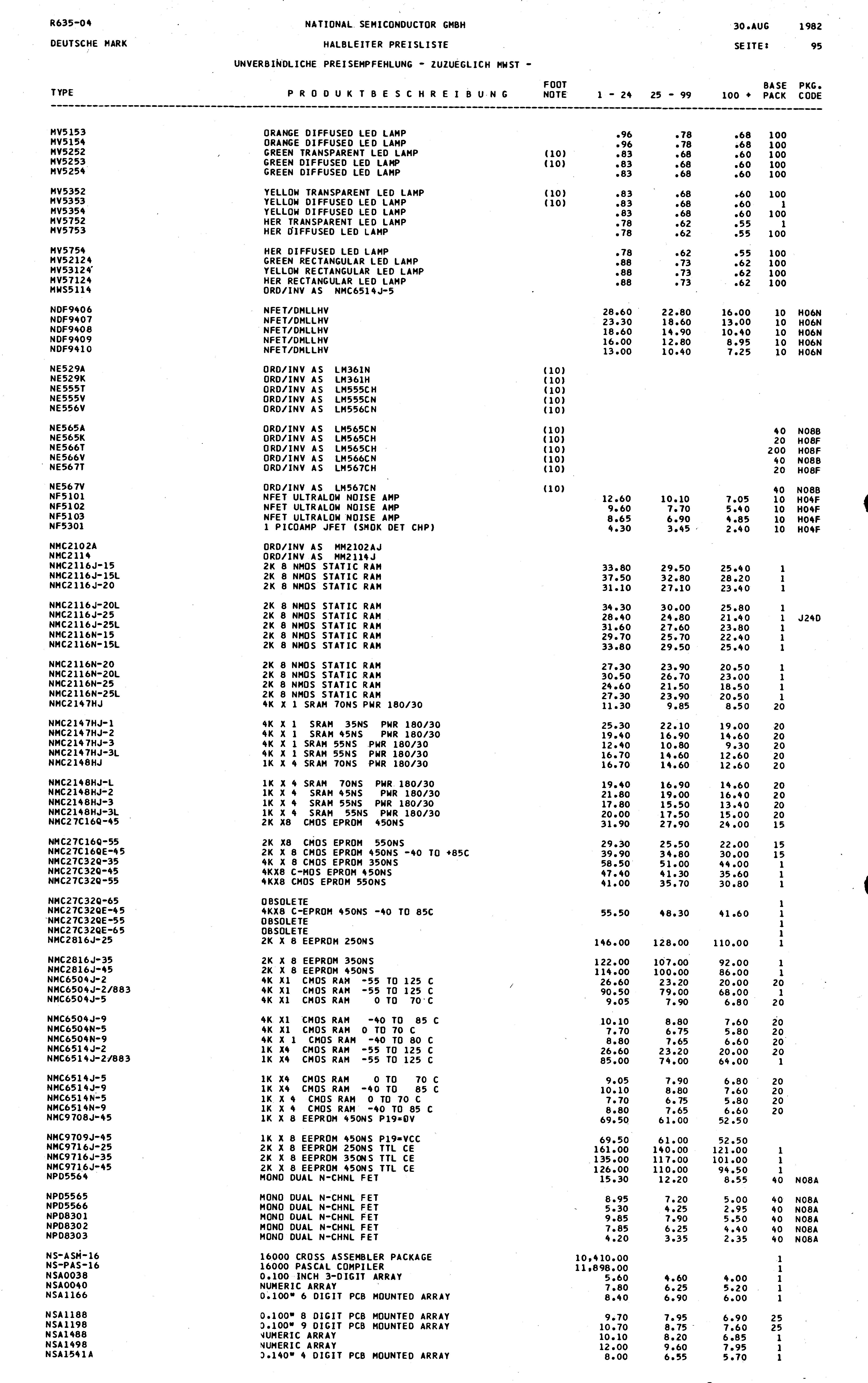
DEUTSCHE SEMICONDUCTOR GMBH SEITE| 95
TYPE FOOT NOTE BASE PKG
NV5153 ORANGE DIFFUSED LED LAMP .96 .78 100
NV5154 ORANGE DIFFUSED LED LAMP .96 .78 100
NV5255 GREEN DIFFUSED LED LAMP .83 .68 100
NV5256 GREEN DIFFUSED LED LAMP .83 .68 100
NV5754 YELLOW TRANSPARENT
0V; VCSD = 5V; VIN= 5V; - - 1 Tj= -40°C...150°C Openload ON-state I current detection VIN= 5V; 5 - 70 mA OL I = 5 µA threshold SENSE Max analog sense V SENSE output voltage IOUT = 18A; RSENSE = 3.9KΩ 5 - - V Analog sense output VSENSEH (2) VCC = 13V; R SENSE = 3.9KΩ - 8 - V voltage in fault condition
; V INV 90 pF SWITCHING Symbol Parameter Test Conditions Min Typ Max Unit d(on) Turn-on Delay Time 70 200 ns VDD=15V; ID=0.5A tr Rise Time V =5V; R =R =330 170 500 ns d(off) Turn-off Delay Time gen gen IN MINn 350 1000 ns (see figure 1) tf Fall Time 200 600 ns d(on) Turn-on Delay Time 0.25 1.0 s VDD=
measurements (PCB: Double layer, Thermal Vias, FR4 area= 77mm x 86mm, PCB thickness=1.6mm, Cu thickness=70µm (front and back side), Copper areas: from minimum pad lay-out to 8cm ). Figure 36. R vs. PCB copper area in open box free air condition (one channel ON) thj-amb RTHj_amb(°C/ W) 70 65 60 55 50 45 40
Vising 5 30 60 µs d(on) (see Figure 5) td(off) Turn-off delay time edge to VOUTo= 11.7 Vlling 10 30 70 )µs (see Figure 5) t ( s R L 6.5 Ω from V OUT = 1.3 V c dV OUT/d(on) Turn-on voltage slopeto VOUT = 10.4 V 0.15 dSeeu 1.5 V/µs (see Figure 5) r o Figure 10 R L 6.5 Ω from VOUT = 11.7 V P dV OUT/d(off

 Bild
Bild
 Bild
Bild
 Bild
Bild
 Bild
Bild