Steampunk Archäologie - Blindflug mit Epson HX-20 Das Thema hat mich animiert, fib.bas von Yalu auf einem 44 Jahre alten Epson HX-20 laufen lassen. Der HX-20 hat einen Hitachi 6301 mit 614kHz. Darauf läuft ein "Microsoft & Epson" Basic von 1982. fib.bas lief abgesehen von RIGHT$ und
Ambienttemperatureoperation(°C) 55 55 55 55 55 55 55 55 55 m r n Ambienttemp. duringstorage/transport(°C) -40 to 85 -40 to 85 -40 to 85 -40 to 85 -40 to 85 -40 to 85 -40 to 85 -40 to 85 -40 to 85 E e IP Class 20 20 20 20 20 20 20 20 20 s l n E Weight (kg) 0.27 0.34 0.28 0.32 0.31 0.31 0.26 0.26 0.43 Connectors
eine Multiplikation bzw. Division und die dürften hier recht häufig genutzt werden. - "RV32E" Base integer instruction set (embedded), 32-bit, 16 registers - "C" Standard extension for compressed instructions - "M" = Standard extension for integer multiplication and division - https://en.wikipedia.org
und imdem man ldexpf verwendet statt *2: Auf AVR dauert float+float ca 100 Cycles, ldexpf kostet ca. 40. Falls man wirklich entsprechende Grafiken möchte, würde man ohnehin auf Fixed-Point gehen. Selbst mit FPU kann das schneller sein als float, und vor allem kann man eine viel bessere Auflösung erreichen
sich überhaupt um "normale" Transistoren? 2N5xxx sind mir auch schon als Bezeichnung für seit über 40 Jahren sehr exotische Halbleiterbauelemente (es gibt "mittlerweile" also 40- 50 Jahren...andere, bessere, "normale" Lösungen) bzw. bei sehr spezielle "Transistoren" (mehr als 3 Schichten bzw. Halbleiterübergänge
keine analogen Fernseher mehr geben wird, kannst du dir den ganzen HF-Kram schenken und einfach das BAS-Signal auf einen Monitor geben, nachdem du die H-Sync und V-Sync Frequenzen auf dessen etwas höheren Frequenzen angepasst hast. Evtl müssen dann die X-Y-Sägezähne auch etwas steiler werden.
evaeu man ~› K am _ _:ßN. 744 1 r @ 3 man mw m_ ` wasnzøøe a-saø a m zsaeå vsaeu vßßf a m a 5 øeaeu . 40ø41a ähm š200? m i _ i .' 3 -1 'X m u g „am K_ _ a W -*_ ezae 2 zsø_uac å X CKman ' anÜ 1? m14 421 ~ Rs4:Esam =ä--§6_ 50 R409- “425__ *7a4 øv-' was S W aa à g samg ecm« 07 00 S, _ . _ sıwms E vøavu40mgW
overvoltages are a concern. > 6. **Packaging:** It uses a **stud-mount package** with a threaded metal base. This design is characteristic of high-power components requiring efficient heat dissipation, as the base is intended to be mounted onto a heatsink. The braided wire lead serves as one of the electrical
a wired output (the clear/transparent cable) > - Color: Green plastic/polymer housing with metal base > - Application: Used for pressure monitoring in industrial systems, hydraulic equipment, or similar applications > This type of sensor would convert pressure measurements into electrical signals
Metric) DP20M-11V12 (Metric) 3500 DP20M-07V24 (Metric)) 50 4000 DP20M-11V24 (Metric))60 45 3000 3500 50 40 3000 2500 35 2500 40 2000 30 ) 25 % m 2000 30 % m 1500 A y r A y ( 20 t c ( 1500 t c d 1000 15 e i e 20 e i e r i p 1000 r i S 10 C E S 10 C Ef 500 5 500 0 0 0 0 0 10 20 30 40 50 60 70 0 10 20 30 40
x 1200 = 91.800.000 byte also 87,5Mb die jede Sekunde anfallen ... und... der "SPI" wird mit 40-50MHz getaktet sein
576604#7852430 Er kommt darin auf 90MByte/s meint aber vermutlich 90MBit/s. Und das ist halt für 100Base-TX grenzwertig. Also brauchts einen Controller der ein GBit PHY treiben kann. Der schon vorgeschlagene STM32N6 sollte das schaffen. Daten rein mit PSSI -> DMA raus dann per DMA -> Ethernet. Matthias
periphery modules they belong to - each periphery module (e.g. RCC, GPIOA, GPIOB, USB, …) has its own base address. The addresses of the individual registers are specified as an offset that needs to be added to this base address to obtain the full absolute address of the register. Chapter 7.3.7 specifies
multiply r8 by 4 (since each word is 4 bytes in size) and add it to r7, which contains the array’s base address. At the end of the loop, r8 is compared with 18, which is the number of entries in the array. This variant is actually less efficient, as it needs to keep both the base address and the index
3410 DATASHEET Maximum Ratings T A= 25 °C Parameter Symbol Values Operating temperature T op min. -40 °C max. 100 °C Storage temperature T stg min. -40 °C max. 100 °C Collector-emitter voltage V CE max. 5.5 V Collector current I max. 20 mA C Emitter-collector voltage V max. 0.5 V EC ESD withstand voltage
Temperature Figure 8. I/O Source Current vs Output High Voltage 45 45 V = 5 V V CC= 3.3 V T = 25ºC CC T = −40ºC 40 A 40 A T = −40ºC 35 A 35 T = 25ºC ) A A A 30 ( 30 ( 25 E 25 E R R20 U 20 O S IS15 I 15 TA= 85ºC 10 TA= 85ºC 10 5 5 0 0 0.0 0.1 0.2 0.3 0.4 0.5 0.6 0.7 0.0 0.1 0.2 0.3 0.4 0.5 0.6 0.7 VCC − OH (V
10 40 ns capacitive load of 400 pF] 20 80 ns tfDA fall time of SDAH signal capacitive load from 10 pF to 100 pF 10 80 ns capacitive load of 400 pF] 20 160 ns tSP pulse width of spikes that must be SDAH and
(max) |VO–V |, V = −28V, I o −100 mA 2.5 3.0 V (max) (8) + − PSRR Power Supply Rejection Ratio V = 40V to 20V, V = −40V, 120 85 dB (min) V CM = 0V, o = 0 mA V = 40V, V = −40V to −20V, 105 85 dB (min) V = 0V, I = 0 mA CM o CMRR (8) Common Mode Rejection Ratio V = 60V to 20V, V = −20V to −60V, V = 20V
least 35 m thick) connected to all DRAIN pins of the relative channel. ELECTRICAL CHARACTERISTICS (-40°C < T < 150°C, unless otherwise specified) (Per each device) j OFF Symbol Parameter Test Conditions Min Typ Max Unit Drain-source Clamp VCLAMP VIN=0V; D =0.5A 40 45 55 V Voltage Drain-source Clamp VCLTH
2.900 3.500 ddd 0.100 30/34 VND5E160J-E Package and packing information 5.3 Packing information Figure 40. PowerSSO-12 tube shipment (no suffix) Base Q.ty 100 B C Bulk Q.ty 2000 Tube length (± 0.5) 532 A 1.85 A B 6.75 C (± 0.1) 0.6 All dimensions are in mm. Figure 41. PowerSSO-12 tape and reel shipment (suffix “TR”) REEL DIMENSIONS Base Q.ty 2500 Bulk Q.ty 2500 A (max) 330 B (min) 1.5 C (± 0.2) 13 F 20.2 G (+ 2 / -0) 12.4 N (min) 60 T (max) 18.4 TAPE DIMENSIONS According to Electronic Industries Association (EIA) Standard 481 rev.
5750 j I = 10 A; V = 4 V; dK 2K 2 Current sense ratio driftUT SENSE -8 +8 % T j -40 °C...150 °C IOUT = 30 A; SENSE = 4 V; K I /I T = -40 °C 4200 4900 5500 3 OUT SENSE j T j 25 °C...150 °C 4400 4900 5250 IOUT = 30 A; SENSE = 4 V; dK 3/K3 Current sense ratio driT = -40 °C...150 °C -6
Manuel S. schrieb im Beitrag #7846541: > 3 phase pfc wie Base64 U. geschrieben hat. > Das ist glaub am vielversprechendsten. > Solche dinger gibts vom China Mann schon unter 50€, haben einen 0-5V Ist zwar technisch absolut machbar, aber so wie dein Erfahrungsschatz
Base64 U. schrieb im Beitrag #7846778: > Gerade in solchen Stressigen Situationen zahlen sich einfache, robuste > Lösungen aus. ACK.
nach Geschwindigkeit und Resonanz der uC machen. > Der Motor ist ein 17 HS 4401 D Fehler 2. 40Ncm, was erwartest du da für ein Drehmoment, hoher Wicklungswiderstand, hohe Induktivität was erwartest du da für ein Tempo, 5.7V hoher Spannungsbedarf. 1.5Arms Nennstrom mit einem Treiber der keine
. Ist das zwingend erforderlich? Tatsächlich sind mir 200 Schritte mehr als genug > Fehler 2. 40Ncm, was erwartest du da für ein Drehmoment, Nun, um die 40 Ncm. An der Aufgabe gemessen würden mir sogar die Hälfte reichen. > Fehler 3. Nur Wave-Betrieb. Ließe sich das etwas genauer erklären?
S p a d m a M g s C m m y t f - o m c O N F R D I A C C C E I P ( T P EFM8UB20F64G-B-QFP48 64 4352 40 32 5 5 Yes Yes Yes -40 to +85 °CQFP48 EFM8UB20F64G-B-QFP32 64 4352 25 20 5 4 — — Yes -40 to +85 °CQFP32 EFM8UB20F64G-B-QFN32 64 4352 25 20 5 4 — — Yes -40 to +85 °CQFN32 EFM8UB20F32G-B-QFP48 32 2304 40 32 5 5 Yes Yes Yes -40 to +85 °CQFP48 EFM8UB20F32G-B-QFP32 32 2304 25 20 5 4 — — Yes -40 to +85 °CQFP32 EFM8UB20F32G-B-QFN32 32 2304 25 20 5 4 — — Yes -40 to +85 °CQFN32 silabs.com | Smart. Connected
HCPL- Min. Typ.a Max. Unit Test Conditions Fig. Note Current Transfer Ratio CTR 800 3500 25k % IF=40μA,V CC = V O 0.4V 3, 4 b 4.5V 600 3000 8k IF=0.5mA, V CC = 4.5V 700 3200 25k IF= 40 μA 500 2700 8k IF= 0.5 mA Logic Low Output Voltage VOL — 0.06 0.4 V IF= 40 μA, O = 280 μA 1, 2 — 0.04 0.4 I = 0.5mA
is available in the 14-pin HTSSOP package, and – Digital TV power supply designed to operate from –40°C to 85°C. ™ – High definition Blu-ray Disc players Device Information – Networking home terminal – Digital set top box (STB) PART NUMBER PACKAGE BODY SIZE TPS54525 HTSSOP 5.00 mm × 6.40 mm TPS54525
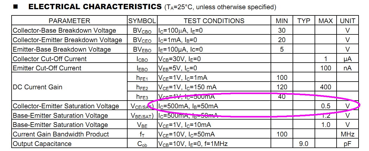
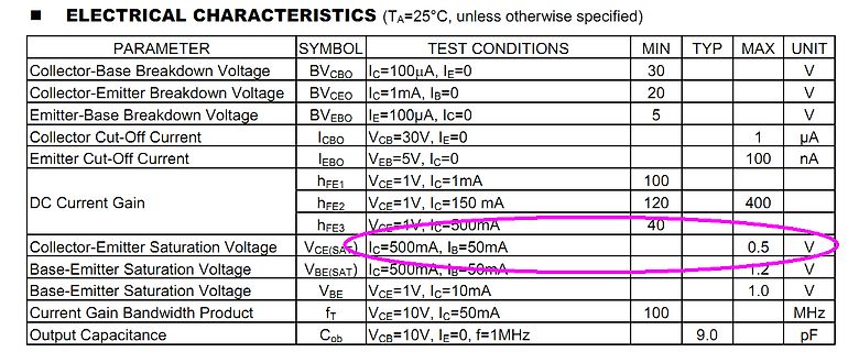
(TA=25°C, unless otherwise specified)
PARAMETER SYMBOL TEST CONDITIONS MIN TYP MAX UNIT
Collector-Base Breakdown Voltage BVcbo Ic=100uA, IE=0 30 V
Collector-Emitter Breakdown Voltage BVceo Ic=1mA, IB=0 20 V
Emitter-Base Breakdown Voltage BVEBO IE=100uA, Ic=0 5 V
Collector Cut-Off Current Icbo VCB=30V
Symbol min max unit note 供电电压 Input voltage V DD -0.3 4.5 V 管脚电流 Pin current nto -100 100 mA 储存温度 Tst -40 85 ℃ Storage temp 工作条件(T=25℃) Working Condition: 参 数 符号 最小值 典型值 最大值 单位 备注 Parameter Symbol min typical max unit note 工作电压 working voltage VDD 2.7 3.3 3.7 V 工作电流 IDD 10 UA 3.3V\25° working current 灵敏度阈值
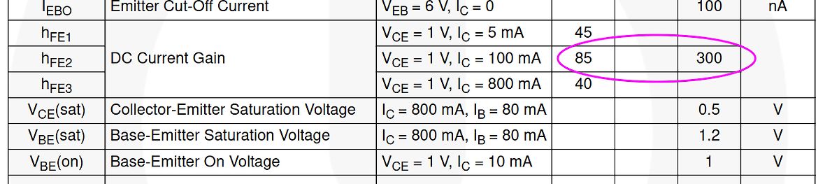
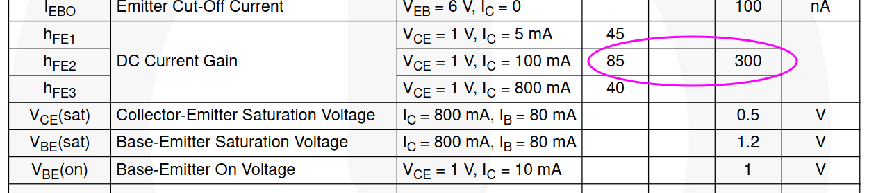
1 V, IC = 5 mA 45
hFE2 DC Current Gain VECE = 1 V, IC = 100 mA 85 300
hFE3 VECE = 1 V, IC = 800 mA 40
VCE(sat) Collector-Emitter Saturation Voltage IC = 800 mA, IB = 80 mA 0.5 V
VBE(sat) Base-Emitter Saturation Voltage IC = 800 mA, IB = 80 mA 1.2 V
VBE(on) Base-Emitter On Voltage VECE = 1 V, IC = 10
Daten: - Maximum DC Current Gain (hFE) is 400 - Continuous Collector current (IC) is 700mA - Base- Emitter Voltage (VBE) is 5V - Collector-Emitter Voltage (VCE) is 20V - Collector-Base Voltage (VCB) is 30V Die Lampe läuft mit 5V/250mA. Der Output des PIR Sensors ist 3,3V Meine Berechnungen
Beitrag #7838169: > dort wird OUT über 10k mit dem Gate eines 2N7002 Wir haben hier aber nur Basen zur Verfügung ...
) Input Signal Amplitude (mV) 82 100 80 90 ) (78 o 80 a R B i ( o76 R 70 o S l n i74 60 S 72 50 70 40 -40 -20 0 20 40 60 80 100 120 3.0 3.5 4.0 4.5 5.0 5.5 Temperature (C) VDDA Supply (V) SNR Si8931 Si8932 Figure 11. Signal-to-Noise Ratio (dB) vs. Temperature (°C) Figure 12. Signal-to-Noise Ratio (dB
news/studie-e-zigaretten-loesen-potenziell-schaedliche-immunreaktionen-in-der-lunge-aus-6f2ebfe3-8623-40e9-be5a-93a43ca34078 Schön. Den Teufel mit dem Belzebub austreiben. Bevor Du fragst: Ich habe 30J geraucht und habe vor dem Schlaganfall aufgehört. Das dicke Ende kommt aber vielleicht noch.
0.00 16:57:39.169 -> 2.00 16:57:39.169 -> IWDG Refreshed. 16:57:39.666 -> IWDG Refreshed. 16:57:40.162 -> IWDG Refreshed. 16:57:40.659 -> IWDG Refreshed. [/code] Bild kommt auch gleich noch eins. ;)
6.3 Ordering Information Ordering code format MSiXXXX-PPP-T-FF XXXX Part Number PPP Package Type Q40 6 x 6 mm QFN 40 pin T Temperature Range C Commercial (-20 to +85 °C) FF Finishing Form DS Dry pack Trays DT Dry pack tape and reel NS Non-Dry pack Trays NT Non- Dry pack tape and reel Table 34: Ordering Information Code Description MSi001-Q40-C-DS MSi001 Dry pack trays MSi001-Q40-C-DT MSi001 Dry pack tape and reel R3v2.0 Mirics Confidential 24 MSi001 For more information contact: Mirics Semiconductor Inc info@mirics.com Oakmere, Barley Way
SN Level-3-260C-168 HR -40 to 125 LM2574M -ADJ P+ Samples LM2574N-12/NOPB ACTIVE PDIP P 8 40 RoHS & Green NIPDAU Level-1-NA-UNLIM -40 to 125 LM2574N -12 P+ Samples LM2574N-3.3/NOPB ACTIVE PDIP P 8 40 RoHS & Green NIPDAU Level-1-NA-UNLIM -40 to 125 LM2574N Samples -3.3 P+ LM2574N-5.0/NOPB ACTIVE PDIP P 8 40 RoHS & Green NIPDAU Level-1-NA-UNLIM -40 to 125 LM2574N Samples -5.0 P+ LM2574N-ADJ/NOPB ACTIVE PDIP P 8 40 RoHS & Green NIPDAU Level
bythevoltageontheV pin(C1’soutput).V drivestCe A series RC from V C to ground provides the necessary base of Q1. As the V Coltage rises, Q2 conducts less pole-zero combination. current, resulting in less drop across R5. Q4’s peak The LT1302-5 incorporates feedback resistors R1 and current must then increase
Noch mal eine GNSS Messung von heute über ca. 40 Minuten, diesmal mit zwei GNSS Empfängern an zwei festen Punkten (Abstand ca. 50 Meter) mit SAPOS-HEPS Korrekturdaten und zusätzlich der Abstand zwischen den Empfängern wenn die beiden GNSS Empfänger als Base und Rover verwendet werden (also die Base die Korrekturdaten liefert). Sonst fast alles wie bei der Messung weiter oben, diesmal bei guter Rundumsicht und Bewölkung. Die Bilder im Anhang zeigen
bythevoltageontheV pin(C1’soutput).V drivestCe A series RC from V C to ground provides the necessary base of Q1. As the V Coltage rises, Q2 conducts less pole-zero combination. current, resulting in less drop across R5. Q4’s peak The LT1302-5 incorporates feedback resistors R1 and current must then increase

 Bild
Bild
 Bild
Bild
 Bild
Bild