over recommended operating conditions (unless otherwise noted) PARAMETER TEST CONDITIONS MIN TYP † MAX UNIT VIT+ Positive-going input threshold voltage 750 900 mV See Table 1 VIT– Negative-going input threshold voltage 500 650 mV Vhys Hysteresis voltage IT+ – IT–) 100 VOH High-level output voltage –6
funktionieren und auch für das ADC-Triggersignal. Aber der ADC selbst benutzt einen "normalen" Takt mit max. 60 MHz und mit dem muss der Trigger synchronisiert werden. Für die Abtastzeitpunkte bleibt die Auflösung also bei 16.7 ns. Das sollte aber kein Problem sein, solange du das Signal mit hoher Auflösung
Prescaler auf 1 steht. Dann muss alles noch durch die Matrix und auf den Ausgang. Die Ausgänge können max. 180MHz bei 10pf Last und das mit einer Rise/Fall Time von 1,7ns. Das mit dem Ram wäre kein Problem der Chip hat FSMC und kann externes Ram ansteuern.
the counter is full (therefore the counter is also presettable for the DOWN-phase to get a defined max. DOWN-timing in case of a fault). When the DOWN-phase is ready, the contents of the counter is transferred to the output shiftregister and the AZ-phase is started. The timing of the AZ~phase is done
zusammen benutzen kann. https://www.techpowerup.com/gpu-specs/tesla-m10.c3035 Der AMD Ryzen™ AI Max+ PRO 395 macht so um die 200GB/s auf dem Speicher und man kann eben 128GB RAM reinmachen. Allerdings kostet so ein komplett neues System natürlich auch sehr viel mehr als 200€ für eine M10.
Qwen3-coder-next 80B sollte eigentlich komfortabel auf deinen RTX-Stack passen. Achte auf ein max. Kontextfenster. Viel Spass beim Agent-Tuning ;)
types o 2.54mm pitch, 7.5mm long standard o 2.00mm pitch, 3.68mm long low profile • Component heights max. 1.4mm on connector side max. 1.4mm on flash side • Weight (max.) 5g Figure 2: Mechanical Dimensions for U-500 1GB-4GB drive Figure 3: Mechanical Dimensions for U-500 8GB-32GB drives All dimensions
, y a PARTNUMBER/STANDARDCONFIGURATIONS W a Numberof “A” “B” “C” y (10,16) “A” PartNumber Contacts Max. Max. Max. R Max. Max. 1.100 .900 .700 3 514-AG21D 14 (27,49) (22,86) (17,78) 2 . 1.220 1.010 .800 n “C” (2,54) “B” 516-AG21D 16 (30,99) (25,65) (20,32) , Max. Typ. Max. g r e i Note: Before ordering
Lead–free assembly p P -Temperature Min (T s(min) 150°C Ramp-up Critical Zone TLtoPT Pre Heat -Temperature Max (T s(max) 200°C L tL T -Time (min to max) (s ) 60 – 180 secs es(max) t Average ramp up rate (LiquidusTemp (T )A e Ramp-down 3°C/second max ps(min) to peak e Preheat T T S(max)T A Ramp-up Rate 3°C/second
Specificationsas defined by Philips. 11/14 TDA7313 SO28PACKAGE MECHANICAL DATA mm inch DIM. MIN. TYP. MAX. MIN. TYP. MAX. A 2.65 0.104 a1 0.1 0.3 0.004 0.012 b 0.35 0.49 0.014 0.019 b1 0.23 0.32 0.009 0.013 C 0.5 0.020 c1 45⋅ (typ.) D 17.7 18.1 0.697 0.713 E 10 10.65 0.394 0.419 e 1.27 0.050 e3 16.51 0.65 F 7.4 7.6 0.291 0.299 L 0.4 1.27 0.016 0.050 S 8⋅ (max.) 12/14 TDA7313 DIP28 PACKAGE MECHANICAL DATA DIM. mm inch MIN. TYP. MAX. MIN. TYP. MAX. a1 0.63 0.025 b 0.45 0.018 b1 0.23 0.31 0.009 0.012 b2 1.27 0.050 D 37.34 1.470 E 15.2 16.68 0.598 0.657 e 2.54
and V ds being the intrinsic drain-source voltage. The charge and capacitances are: for V > V new max 168 V max Vnew − V max Q gs = Cgs0· 2·Vbi 1 − 1 − + (11.364) V bi 1 − VVax bi ∂Q gs C gs0 ∂Vnew = · (11.365) ∂Vgs 1 − VVax ∂V gs bi ∂Q gs C gs0 ∂Vnew = · (11.366) ∂Vgd 1 − VVax ∂V gd bi and
: 74h Size: 8 bits Table 3-213 Lock Count Bit Access Symbol Description [7:4] R/W locked_cnt_noisy_max These bits set the max value of the hlock sensor for noisy signals. 8 is added to this value. Default = 7 stands for 15. These bits set the max value of the hlock sensor for clean signals. 8 is [3:0] R/W locked_cnt_clean_max added to this value. Default = 4 stands for 12. 3.9.18 H Loop Max State Address Offset: 17h Access: Read/Write Default Value: CBh Size: 8 bits 83 电子专业技术主页: HTTP://WWW.LCDHOME.NET 资料收藏: 版权归原作者所有 谨供学习用
900 D *RoHSDirective2015/863,Mar31,2015andAnnex. “-RC”su xindicatesRoHScompliance. 0.138 0.236 45° 0.394 Core Dimension 0.024 0.55 Max. 1.5 Fig. A Fig. B Fig. C Fig. D Dimensions: Inches WARNING Cancer and Reproductive Harm www.P65Warnings.ca.gov Specifications are subject to change without notice. Users
IRLZ44NPBF ELECTRONICS CO.,LTD N-Channel Enhancement Mode MOSFET Package Information TO-220 SYMBOL MIN NOM MAX MIN NOM MAX A 4.40 4.57 4.70 0.173 0.180 0.185 A1 1.27 1.30 1.33 0.050 0.051 0.052 A2 2.35 2.40 2.50 0.093 0.094 0.098 b 0.77 0.80 0.90 0.030 0.031 0.035 b2 1.17 1.27 1.36 0.046 0.050 0.054 c 0.48 0.50
define the switching frequency fmax above which the L6599 will enter burst-mode operation. Once fixed f max, RF max will be found from the relationship: 3 RF min RF max = 8-⋅f----------------- --------- – 1 fmin Note that, unlike the max considered in the previous section ("Chapter 7.1: Oscillator"), here
be left unconnected while XTAL1 is driven, as shown in Figure 3. Figure 2. Oscillator Connections MAX 1 HC BUFFER HC C2 XTAL2 C1 XTAL1 GND Note: When using the MCU Oscillator as a clock for an external device, an HC buffer should be connected as indicated in the figure. Figure 3. External Clock Drive
20 A1, Frequenz- Smart PLGS 2012 A1. leistung.......≤20dBm Frequenzband ..2400-2483,5MHz Temperatur.max 50 °C Ladevorgang 0 - 10 °C, bzw. 50 - 60 °C bei einem Ladestrom von max. 4 A 10 - 50 °C bei einem Ladestrom von max. 12 A Betrieb......-20 - 50 °C Lagerung 8 DE AT CH Ladezeit Akku Smart PAPS 208 A1
VAC breakdow3 Between open contact 350 Vrms (500 V DC) voltage* Between contact and coil 1,000 Vrms Max. switching power 33 VA, 20 W 4 Rating Max. switching voltage 110 V AC, 30 V DC Operate time* (at nominal voltage) Max. 3 ms (Approx. 1 ms) Release time(without diode)* 4 (resistive) Max. switching current
place.The compressors will withstand storage temperatures down to -35°C. Condensing temperatures: Max. 60°C at stable conditions and max. 70°C at peak load. Ambient temperatures: Min. -10°C, max. 55°C The BD compressor concept includes an electronic unit which features overload protection, battery protection
specification 2 Remote 8-bit I/O expander for I C-bus PCF8574 SYMBOL PARAMETER CONDITIONS MIN. TYP. MAX. UNIT I/Os VIL LOW level input voltage −0.5 − +0.3VDD V VIH HIGH level input voltage 0.7VDD − VDD + 0.5 V IHL(max) maximum allowed input VI≥ VDD or I ≤ SS − − ±400 A current through protection diode
ist voll mit VCO Schaltungen aus der Analog-Synthesizer (Moog) Zeit. Evtl. reicht dir ja auch ein MAX038?
Axel S. schrieb im Beitrag #7839651: > Evtl. reicht dir ja auch ein MAX038? Den MAX038 habe ich schon lange nicht mehr gesehen. War wohl zu teuer. Ausserdem geht er bis zu weit höheren Frequenzen, was hier nicht gebraucht wird. Wolfgang D. schrieb im Beitrag #7839692
the or switched-mode power supply. XLamp XM-L have multi-ampere Within specification boundaries, 1 max-current specifications. none of these conditions is cause However, to explore the limits of for concern in the long-term lumen the possible, but not necessar- maintenance or reliability of the ily reasonable
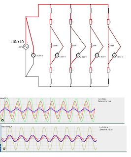
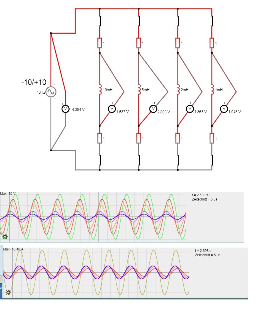
-10/+10 40Hz -4.394 V 1 10mH 1 1.687 V 1 5mH 1 2.803 V 1 2mH 1 1.863 V 1 1mH 1 1.043 V Max=10 V t = 2.698 s Zeitschritt = 5 µs Max=16.48 A t = 2.698 s Zeitschritt = 5 µs
CHARACTERISTICS TA= 25°C, VCM = 0V unless otherwise noted. SYMBOL PARAMETER CONDITIONS VSUPPLY MIN TYP MAX UNITS VOS Input Offset Voltage ±15V 0.2 0.6 mV ±5V 0.2 0.6 mV ±2.5V 0.3 0.8 mV IOS Input Offset Current ±2.5V to ±15V 40 120 nA IB Input Bias Current ±2.5V to ±15V 120 500 nA en Input Noise Voltage
VAC breakdow3 Between open contact 350 Vrms (500 V DC) voltage* Between contact and coil 1,000 Vrms Max. switching power 33 VA, 20 W 4 Rating Max. switching voltage 110 V AC, 30 V DC Operate time* (at nominal voltage) Max. 3 ms (Approx. 1 ms) Release time(without diode)* 4 (resistive) Max. switching current
be left unconnected while XTAL1 is driven, as shown in Figure 3. Figure 2. Oscillator Connections MAX 1 HC BUFFER HC C2 XTAL2 C1 XTAL1 GND Note: When using the MCU Oscillator as a clock for an external device, an HC buffer should be connected as indicated in the figure. Figure 3. External Clock Drive
sieht heftig aus, Gas und Kohle rennen fast am derzeit verfügbaren Limit, Grenzkuppelstellen können max. 20GW (wenn wir den Saft denn überhaupt kriegen), es fehlen aber >21GW. Woher kommt der Rest? Das soll jetzt keine polemisch/politische Diskussion werden was alles gut/richtig oder schlecht/falsch
Hallo H.Joachim S., H.Joachim S. schrieb im Beitrag #7790433: > Grenzkuppelstellen können max. 20GW (wenn wir den Saft denn hast Du dafür eine Quelle? Danke.
Verteilung auf die 2 Fühler. Aber es braucht schon ne hinreichend schnelle Abkühlung. Länger als 5, max. 10 Minuten sollte es von 80 auf 50 Grad nicht dauern. Aufheizen von 50 auf 80 Grad in < 1 Minute. Aber da kann man ja vom Widerstand ne Kühlfahne durch die Isolierung legen und nach Tests dann
im Speicher verglichen. Jeweils ein einstellbares Delta für an/aus, aus bei Speicher oder Kollektor max., beide einstellbar. Zusätzlich ist die Pumpe evtl. PWM gesteuert. Da wird es dann komplizierter. Ein Flow Sensor könnte ausgewertet werden für Ertragsanzeige. Für den Betrieb ist das aber nicht
85 ℃ Storage Temperature Tstg -40~ +85 ℃ Lead Soldering Temperature Tsol 26℃ /10sec - *Pulse width Max 0.1ms, Duty ratio max 1/10 ■ Electrical -Optical Characteristics (Ta=25℃) V FV) R (µA) Iv(mcd) λD(nm) 2θ1/2(deg) Part Number Color Min. Typ. Max. Max. Min. Typ. Max. Min. Typ. Max. Typ. F =5mA V R5V
output impedance.IC to the active area + 1/160 1/12 7.93% e 6.3% 5.7% In addition, please limit the min-max spread of RC decay to 1/160 1/11 7.77% 6.2% 5.6% be: f i | RC MAX– RC MIN | < 0.15 S VIDEO CSTN & COG applications. For LCM with r ft = 180mS ~ 200mS or smaller, bottom of the screen are uniform.e top
(ground = 0 V). Symbol Parameter Conditions 25 °C -40 °C to +85 °C -40 °C to +125 °C Unit Min Typ Max Min Max Min Max VIH HIGH-level V CC = 2.0 V 1.5 1.2 - 1.5 - 1.5 - V input voltage V CC = 4.5 V 3.15 2.4 - 3.15 - 3.15 - V V = 6.0 V 4.2 3.2 - 4.2 - 4.2 - V CC VIL LOW-level V CC = 2.0 V - 0.8 0.5 -
(ground = 0 V). Symbol Parameter Conditions 25 °C -40 °C to +85 °C -40 °C to +125 °C Unit Min Typ Max Min Max Min Max V HIGH-level V = 4.5 V to 5.5 V 2.0 1.6 - 2.0 - 2.0 - V IH CC input voltage V LOW-level V = 4.5 V to 5.5 V - 1.2 0.8 - 0.8 - 0.8 V IL CC input voltage V HIGH-level V = V or V ; V = 4.5
https://www.analog.com/media/en/technical-documentation/data-sheets/MAX7219-MAX7221.pdf#page=12 Das ist aber nur für 2 Digits gezeichnet, für acht braucht man den MAX394 und die Transistoren noch dreimal. Es wird ziemlich aufwendig, wäre es nicht besser, entweder einen
> Im Datenblatt ist ein Beispiel für höhere Spannung Auf Seite 12 werden mit einem Analogschalter MAX394 zwei Ausgänge DIG0 und DIG1 im Pegel von 0 V auf -5V umgesetzt, der reicht nicht für 8 Stellen.
which has two extreme values along the hysteresis curve Bx,1− B x,2 B x,1− B x,2 µmin = min , and µ max = max . (5.58) H x,1Hx,2H x,1− H x,2 Hx,1,Hx,2H x,1− H x,2 Hereµ min andµ max aretheminimumandmaximumslopeofthehysteresischaracteristics. The inequality µmin ≤ µ ≤ µ max (5.59) is obvious, from which
Doppeltransistor. Die beiden Systeme sind dann nicht explizit gematcht (wie bei einem MAT02 oder LM394), aber da sie auf dem Wafer direkt nebeneinander gesessen haben, sind ihre Eigenschaften sehr ähnlich.
------- Ich kann das Alter nicht nachvollziehen, schätze die TO-18 / TO-5 mit Gold auf 70er / max. Anfang 80er Jahre.

 Bild
Bild