-
Datei
hardware_t.cpp
3; CH2_DAC_Correction_1_bak = CH2_DAC_Correction_1; CH2_DAC_Correction_2_bak = CH2_DAC_Correction_2; CH2_DAC_Correction_3_bak = CH2_DAC_Correction_3; CH3_DAC_Correction_1_bak = CH3_DAC_Correction_1; CH3_DAC_Correction
in „Wittig(welec) DSO W20xxA Open Source Firmware“ · Mikrocontroller und Digitale Elektronik ·
-
Datei
UserInterfaceClass.h
typedef enum { DAC_CH0, DAC_CH1, DAC_CH2, DAC_CH3, DAC_MAX_Channel_nbr } DAC_Channel_t; /** * @brief Public UserInterface class definition */ typedef struct CUI_t *CUI; /** * @brief UserInterface class parameters definition
in „STM32 PMSM FOC set Speed in rpm“ · Mikrocontroller und Digitale Elektronik ·
-
PDF
A3967-Datasheet.pdf
Angle Full Step Half Step ¼ Step ǩ Step (%Itripx) (%Itripx) (º) (%) (%) 1 1 1 100.00 0.00 0.0 2 98.08 19.51 11.3 2 3 92.39 38.27 22.5 4 83.15 55.56 33.8 1 2 3 5 70.71 70.71 45.0 6 55.56 83.15 56.3 4 7 38.27 92.39 67.5 8 19.51 98.08 78.8 3 5 9 0.00 100.00 90.0 10 –19.51 98.08 101.3 6 11 –38.27 92.39 112.5
in „Vref Dual Step Motor Shield (Arduino) iteadstudio.com“ · Mikrocontroller und Digitale Elektronik ·
-
PDF
GD32VF103_Datasheet_Rev1.0.pdf
with Ro buffer OFF — — — 15 kΩ No pin/pad capacitance CLOAD(2) Load capacitance — — 50 pF included DAC_OUT Lower DAC_OUT voltage (2) — 0.2 — — V min with buffer ON DAC_OUT Higher DAC_OUT voltage VDDA- max(2) with buffer ON — — — 0.2 V DAC_OUT Lower DAC_OUT voltage — — 0.5 — mV min(2) with buffer OFF
in „RISC-V: Wird das was?“ · Mikrocontroller und Digitale Elektronik ·
-
PDF
GD32VF103_Datasheet_Rev1.0.pdf
with Ro buffer OFF — — — 15 kΩ No pin/pad capacitance CLOAD(2) Load capacitance — — 50 pF included DAC_OUT Lower DAC_OUT voltage (2) — 0.2 — — V min with buffer ON DAC_OUT Higher DAC_OUT voltage VDDA- max(2) with buffer ON — — — 0.2 V DAC_OUT Lower DAC_OUT voltage — — 0.5 — mV min(2) with buffer OFF
in „STM32F103C8T6 => GD32VF103C8T6“ · Mikrocontroller und Digitale Elektronik ·
-
PDF
tlc5620.pdf
DIGITAL-TO-ANALOG CONVERTERS SLAS081E – NOVEMBER 1994 – REVISED NOVEMBER 2001 functional block diagram 2 REFA + – DAC + 12 8 8 × 2 – DACA Latch Latch 3 REFB + – DAC + 11 DACB 8 Latch Latch 8 × 2 – 4 REFC + – DAC + 10 8 8 × 2 DACC Latch Latch – 5 REFD + – DAC + 9 DACD 8 Latch Latch 8 × 2 – CLK 7 6 Serial Power-On DATA
in „DAC Schieberegister“ · Mikrocontroller und Digitale Elektronik ·
-
PDF
DAC80.pdf
INFORMATION MILS (0.001") MILLIMETERS Die Size 118 x 121 ± 5 3.0 x 3.07 ± 0.13 Die Thickness 20 ± 3 0.51 ± 0.08 Min. Pad Size 4 x 4 0.10 x 0.10 DAC80KD-V DIE TOPOGRAPHY Metalization Aluminum PAD FUNCTION PAD FUNCTION 1 Bit 1 (MSB) 15 –VCC 2 Bit 2 16 OUT 3 Bit 3 17 Ref In 4 Bit 4 18 Bipolar Offset 5 Bit 5 19 Scale
in „Ersatz für DAC80 (12-Bit DIGITAL-TO-ANALOG CONVERTERS)“ · Mikrocontroller und Digitale Elektronik ·
-
PDF
infineon-ug-202311-pl52-2312-121012-solid-state-circuit-breaker-reference-design-user-guide-usermanual-en.pdf
TP6 OCD:Fastcomparatoroutput TP7 CH1_ON DAC0 DAC0output DAC1 DAC1output Figure 13showstheapplicationconnectiondiagram.This reference designis designedtosupportresistiveand inductiveloads.Touseamultichannelconfiguration,twoSSCBdevices cancommunicate
in „Leitungsschutzschalter 24VAC“ · Analoge Elektronik und Schaltungstechnik ·
-
PDF
TLC5620.pdf
DIGITAL-TO-ANALOG CONVERTERS SLAS081C – NOVEMBER 1994 – REVISED FEBRUARY 1996 functional block diagram REFA + – DAC + 8 Latch Latch 8 2 – DACA REFB + – DAC + 2 DACB 8 Latch Latch 8 – REFC + – DAC + 8 Latch Latch 8 2 – DACC REFD + – DAC + 2 DACD 8 Latch Latch 8 – CLK DATA Serial Power-On Interface LDAC Reset LOAD
in „DAC Steuerung mittels SPI“ · Mikrocontroller und Digitale Elektronik ·
-
PDF
ADV7175A.pdf
television (Continued on page 11) FUNCTIONAL BLOCK DIAGRAM M TTX TELETEXT L 10 10-BIT INSERTION T DAC DAC D (PIN 27) TTXREQ BLOCK YUV TO I RBG P 10 10-BIT MATRIX L DAC DAC C (PIN 26) VAA E X 10 10-BIT DAC B (PIN 31) R DAC 8 8 ADD 8 INTER- 8 Y 10 COLOR SYNC POLATOR LFILTERS DATA P7–P0 4:2:2 TO YCrCb
-
PDF
Sp3A-DSP-1800A-Starter-Schematic-Rev1.pdf
_1 K21 DAC_B1 DAC_G[0:3] 13 0.1uF IO_L50n_1 G23 DAC_B2 2 R39 10R0 IO_L51p_1 DAC_B3 B IO_L51n_1 G24 DAC_R0 1 2 B IO_L53p_1 L20 DAC_B[0:3] 13 IO_L53n_1 K20 DAC_R1 FPGA_RS232_Tx IO_L54p_1 F25 DAC_R2 F24 DAC_R3 +3.3V
in „Schematics von Spartan 3A-DSP 1800 Board“ · FPGA, VHDL & Co. ·
-
Datei
tn816def.inc
ADC input pin 6 .equ ADC_MUXPOS_AIN7_gc = (0x07<<0) ; ADC input pin 7 .equ ADC_MUXPOS_AIN8_gc = (0x08<<0) ; ADC input pin 8 .equ ADC_MUXPOS_AIN9_gc = (0x09<<0) ; ADC input pin 9 .equ ADC_MUXPOS_AIN10_gc = (0x0A<<0) ; ADC input pin 10 .equ ADC_MUXPOS_AIN11_gc = (0x0B<<0) ; ADC input pin 11 .equ ADC_MUXPOS_DAC0
in „ATtiny816 wo finde ich def.inc“ · Mikrocontroller und Digitale Elektronik ·
-
PDF
Forum.PDF
Aussortieren_Vor Win10\..\Compute Moen3+B.yS:chDoc 1 2 3 4 1 2 3 4 A A +12 B B CO2dc Pc U1_ ac I2C NLIC0IC0 L U2_dac MCP6H01T-E/OT POI20SD SCL I2Cs.I2C0.SDA PI4a0 SCL PU0c4 1 SDA PI2a0SDA 1 3 P1d0 P 6 VOUT PI2d0 PU0c3 CR1_dac PI2a0A0 10k 1% 1206 P P4 3 2 Pc P J1_da PI2a0VDD VSSPI2d0 691231510004 +3.3 MCP4725A0T-E/
in „Raspberry Pi Compute Module 3 (Carrier Board)“ · Mikrocontroller und Digitale Elektronik ·
-
 Bild
Bild
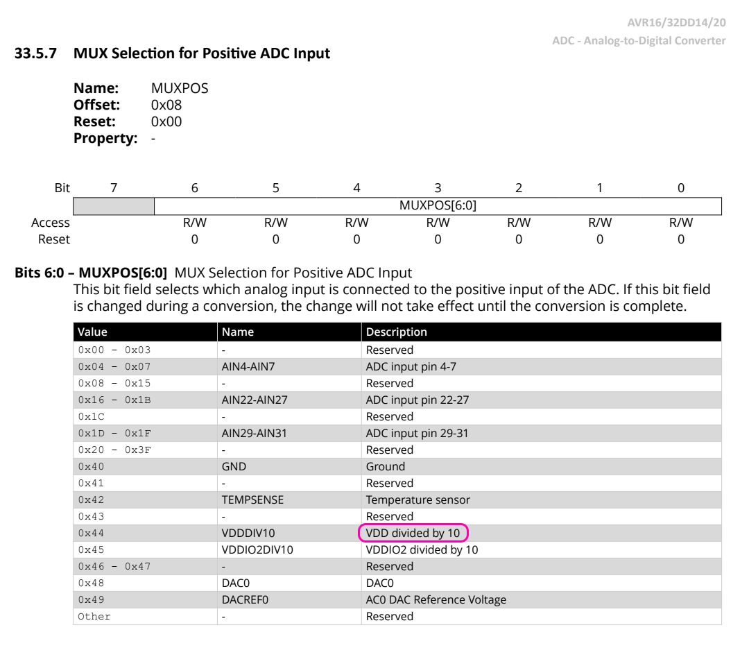
Datenblatt Ausschnitt MUX Selection für ADC Input
0x04 - 0x07 AIN4-AIN7 ADC input pin 4-7 0x08 - 0x15 - Reserved 0x16 - 0x1B AIN22-AIN27 ADC input pin 22-27 0x1C - Reserved 0x1D - 0x1F AIN29-AIN31 ADC input pin 29-31 0x20 - 0x3F - Reserved 0x40 GND Ground 0x41 - Reserved 0x42 TEMPSENSE Temperature
in „neue AVR-µCs: Entwicklungsumgebung“ · Mikrocontroller und Digitale Elektronik · · Screenshots
-
Datei
Programm.txt.txt
// Stop WDT BCSCTL1 |= XTS; // XT = HF XTAL ADC12CTL0 = !REF2_5V + REFON; // Internal 1.5V ref on DAC12_0CTL = DAC12IR + DAC12AMP_5 +DAC12ENC; // internal reference gain 1 encode P1SEL &= 0xDF; // Ausgang für Hintergrund P1DIR |= 0x20; // Ausgang für Hintergrund P5SEL = 0x00; // Ausgänge für LCD P5DIR
in „LCD Display Seriell Ansteuern“ · Mikrocontroller und Digitale Elektronik ·
-
PDF
TLC5620CN_DIP14.pdf
DIGITAL-TO-ANALOG CONVERTERS SLAS081E – NOVEMBER 1994 – REVISED NOVEMBER 2001 functional block diagram 2 REFA + – DAC + 12 8 8 × 2 – DACA Latch Latch 3 REFB + – DAC + 11 DACB 8 Latch Latch 8 × 2 – 4 REFC + – DAC + 10 8 8 × 2 DACC Latch Latch – 5 REFD + – DAC + 9 DACD 8 Latch Latch 8 × 2 – CLK 7 6 Serial Power-On DATA
in „Wie verhält sich der DAC am SPI-Bus (TLC5620)“ · Mikrocontroller und Digitale Elektronik ·
-
Datei
PCM1738.asm
_44100 LDI tmp, 0x08 STS DAC_Deemphasis_freq, tmp .endmacro .macro Set_DAC_Deemphasis_Freq_48000 LDI tmp, 0x04 STS DAC_Deemphasis_freq, tmp .endmacro .macro Set_DAC_Deemphasis_Freq_32000 LDI tmp, 0x0C STS DAC_Deemphasis_freq
in „DAC PCM1738 mode control programmieren“ · Mikrocontroller und Digitale Elektronik ·
-
PDF
515502_1__2_.pdf
DC_CAL 81 31 CAP3 HEADER5x1 /SCS /SCS [3] SW PUSH-SPST NO CAP2 80 GPIO-43 GPIO-42 30 CAP1 GND 24VDC DAC_PWM2 79 GPIO-41 GPIO-40 29 DAC_PWM1 R22 1/10W DAC1 1 DC_CAL EXT_IC-FB GND 100mA 78 GPIO-11 GPIO-10 28 DAC_PWM3 470 5% DAC2 2 1 DC_CAL [3] EXT_IC-FB [6] GPIO-9 GPIO-08 C30 DAC3 2 EN_GATE EXT_IB-FB 77
in „Allgemeine Frage bezüglich Motor Treiber/Inverter“ · Analoge Elektronik und Schaltungstechnik ·
-
PDF
TF5000CI.pdf
by Signal Name I/O Signal Name Ball Number DAC1_AGND1 A8 DAC1_AGND2 C10 DAC1_AVDD0 B6 DAC1_AVDD1 C8 DAC1_AVDD2 A9 DAC1_AVDD3 B11 DAC1_VOUT1 C7 DAC1_CREF_OUT A5 DAC1_VOUT2 B8 DAC1_GREF_OUT A11 DAC1_VOUT3 C11 DAC1_RREF_OUT A7 DAC1_VREF_IN C9 DAC2_AGND0 B17 DAC2_AGND1 B15 DAC2_AGND2 C13 DAC2_AVDD0 C18 DAC2_AVDD1 B16 DAC2_AVDD2 C14 DAC2_AVDD3 A13 DAC2_VOUT1 C17 DAC2_CREF_OUT A19 DAC2_VOUT2 C15 DAC2_GREF_OUT C12 DAC2_VOUT3 B13 DAC2_RREF_OUT A17 DAC2_VREF_IN
in „CPU SAA7219 per Jtag auf Basis FT2232H ansprechen - Tool schreiben“ · PC Hard- und Software ·
-
Datei
04_Ultraschall_HC_SR04_nicht_funktionstuechtig_.c
P5.1 P2.6| // SD-DO |P5.2 P2.5| // SD-CLK |P5.3 P2.4| // |P5.4 P2.3| // |P5.5 P2.2| // |P5.6 P6.7| DAC1 // |P5.7 P6.6| DAC0 // // // - Mai/Juni 2016 //****************************************************************************** #include <msp430x16x.h> unsigned char ZeitOB_A,ZeitUB_A,ZeitOB_B,ZeitUB_B
in „MSP430F1610 und TIMER-B“ · Mikrocontroller und Digitale Elektronik ·
-
Datei
iotn814.h
* ADC input pin 6 */ ADC_MUXPOS_AIN7_gc = (0x07<<0), /* ADC input pin 7 */ ADC_MUXPOS_AIN8_gc = (0x08<<0), /* ADC input pin 8 */ ADC_MUXPOS_AIN9_gc = (0x09<<0), /* ADC input pin 9 */ ADC_MUXPOS_AIN10_gc = (0x0A<<0), /* ADC input pin 10 */ ADC_MUXPOS_AIN11_gc = (0x0B<<0), /* ADC input pin 11 */ ADC_MUXPOS_DAC0
in „Attiny417/814/816/817 und avr-gcc, avr-libc“ · Mikrocontroller und Digitale Elektronik ·
-
PDF
AD9954__DDS_.pdf
consists of a 1 kΩ resistor in series with a 0.1 µF capacitor tied to AVDD. 20 IOUT O Complementary DAC Output. Should be biased through a resistor to AVDD, not AGND. 21 IOUT O DAC Output. Should be biased through a resistor to AVDD, not AGND. 23 DACBP I DAC Biasline Decoupling Pin. 24 DAC_R SET I A resistor
in „DDS-Funktionsgenerator“ · Mikrocontroller und Digitale Elektronik ·
-
Datei
02_Ultraschall_HC_SR04-funktionstuechtig.c
P5.1 P2.6| // SD-DO |P5.2 P2.5| // SD-CLK |P5.3 P2.4| // |P5.4 P2.3| // |P5.5 P2.2| // |P5.6 P6.7| DAC1 // |P5.7 P6.6| DAC0 // // // - Mai/Juni 2016 //****************************************************************************** #include <msp430x16x.h> unsigned char ZeitOB_A,ZeitUB_A,ZeitOB_B,ZeitUB_B
in „MSP430F1610 und TIMER-B“ · Mikrocontroller und Digitale Elektronik ·
-
Datei
main.c
variables uint8_t EEMEM EESleepTime = 64; // Sleep timeout in minutes uint8_t EEMEM EEDACgain = 0; // DAC gain calibration uint8_t EEMEM EEDACoffset = 0; // DAC offset calibration static void Calibrate(void); //static void CalibrateDAC(void); void SimpleADC(void); void ScreenSaver(uint8_t minutes); int
in „ATXmega - Pin Eingang oder Ausgang“ · Mikrocontroller und Digitale Elektronik ·
-
PDF
ak4528vm-en-datasheet.pdf
μs ADC Digital Filter (HPF): Frequency Response (Note 8) −3dB FR 0.9 Hz −0.5dB 2.7 Hz −0.1dB 6.0 Hz DAC Digital Filter: Passband (Note 8) −0.01dB PB 0 20.0 kHz −6.0dB - 22.05 - kHz Stopband SB 24.1 kHz Passband Ripple PR ±0.005 dB Stopband Attenuation SA 75 dB Group Delay (Note 9) GD 30 1/fs DAC Digital
in „Daisy: Eingebettete Plattform für Audioprojekte“ · Mikrocontroller und Digitale Elektronik ·
-
PDF
MP600_DataSheet.pdf
& SDHC with SD 2.0 ), Memory Stick Pro, xD Picture Card ‧ Support multi-block DMA z Embedded Audio DAC & Power Amplifier - Audio DAC - High performance Audio DAC (16bit, 93dB) - Stereo Headphone Driver - Stereo Speaker Amplifier up to 1 Watt (0.5W +0.5W) Revision 0.8 - 2007.03.08 Magic Pixel Confidential
in „Datenblatt von Magic Pixel MP600BUCG“ · Mikrocontroller und Digitale Elektronik ·
-
Datei
MSP3400_ATMEGA32_ADC_2.ino
/ Test/Power: TEST=PB5 // SC‑Out: SC=PD6 // Statusports: LED1=PC3=SUCHLAUF, LED2=PB4=MEMORY // PWM-DAC: PB3 (Timer0), PD7 (Timer2) // ADC: ADC2 (PA2), ADC3 (PA3) // --------------------------------------------------------- #define IR_RECEIVE_PIN PIN_PB2 // PB2 IR-Eingang // Display / Steuer‑Signale #
in „Zeigt her eure Kunstwerke (ab 2023)“ · Projekte & Code ·
-
Datei
MSP3400_ATMEGA32_ADC_2.ino
/ Test/Power: TEST=PB5 // SC‑Out: SC=PD6 // Statusports: LED1=PC3=SUCHLAUF, LED2=PB4=MEMORY // PWM-DAC: PB3 (Timer0), PD7 (Timer2) // ADC: ADC2 (PA2), ADC3 (PA3) // --------------------------------------------------------- #define IR_RECEIVE_PIN PIN_PB2 // PB2 IR-Eingang // Display / Steuer‑Signale #
in „AUDIOCONTROLLER MSP3400C einfach mit ATMEGA32 ansteuern“ · Projekte & Code ·
-
PDF
DS1000Z_Analog.pdf
PIC102 C2 42 VREF_BUF I2 I2 7 21 PIU3010 PIC201 PIC202 6 1K PIU308PIR4201 PIR4202 COR40 COR4 COR5 DAC_TLC274IPWR PIR401 PIR40P2IU309 PIR402 DAC_TLC274IPWR2 PIR501 TLV272IDGK COR3 COR6 R43 10 5 PIR302 PIR301 PIR602 PIR601 1K B R9 8 R7 VCOM_CH2 R10 7 R8 VCOM_CH4 COR41 B VREF_BUF 9 100Ω VREF_BUF 6 100Ω
in „Analogverstärker für Mikrocontroller Oszilloskop“ · Analoge Elektronik und Schaltungstechnik ·
-
PDF
kicad_8450_dcm_liste_neu_v3.pdf
74xgxx.dcm 156 22-05-2017 74xx.dcm 167 22-05-2017 ac-dc.dcm 60 09-07-2017 actel.dcm 18 22-05-2017 adc-dac.dcm 177 08-08-2017 allegro.dcm 29 22-05-2017 Altera.dcm 7 22-05-2017 analog_devices.dcm 24 21-08-2017 analog_switches.dcm 13 22-05-2017 atmel.dcm 495 22-05-2017 audio.dcm 45 07-06-2017 battery_management.dcm
in „KiCAD Eeschema, Bibliotheksdokumentation *.dcm als PDF-Datei“ · Platinen ·
-
PDF
dac8512.pdf
functionality. ORDERINGGUIDE INL Temperature Package Package Model (LSB) Range Description Option DAC8512EP ±1 –40°C to +85°C 8-Pin P-DIP N-8 DAC8512FP ±2 –40°C to +85°C 8-Pin P-DIP N-8 DAC8512FS ±2 –40°C to +85°C 8-Lead SOIC SO-8 DAC8512GBC ±2 +25°C Dice REV. A –3– DAC8512 SDI D11 D10 D9 D8 D7 D6 D5
in „µC soll Strom rausgeben“ · Mikrocontroller und Digitale Elektronik ·
-
PDF
WT588D-U_Voice_Module.pdf
4 NC NC blank 5 NC NC blank 6 NC NC blank 7 RESET RESET Reset pin 8 DAC DAC DAC Audio output pin, need an external amplifier to drive speaker 9 PWM+ PWM+ PWM+ Audio output pin, which can directly drive speaker with the PWM- 10 PWM- PWM- PWM- Audio output pin, which can
in „WT588D Voice Modul Tonqualität“ · Analoge Elektronik und Schaltungstechnik ·
-
PDF
vs1001.pdf
slave co-processor † Operates with single clock 12..13 MHz or oversamplingvariable-sample-ratestereoDAC,fol- 24..26 MHz lowedbyanearphoneamplifierandagroundbuffer. † Low-power operation † On-chip high-quality stereo DAC with no VS1001k receives its input bitstream through a phase error between channels
in „VS1001k: SDI & SCI am SPI-Bus“ · Mikrocontroller und Digitale Elektronik ·
-
Datei
AT90PWM3.xml
ACCESS> <INIT_VAL>0</INIT_VAL> </BIT5> <BIT4> <NAME>DATS0</NAME> <DESCRIPTION>DAC Trigger Selection Bit 0</DESCRIPTION> <TEXT/> <ACCESS>RW</ACCESS> <ENUM>ANALIG_DAC_AUTO_TRIGGER</ENUM> <INIT_VAL>0</INIT_VAL> </BIT4> <BIT2> <NAME>DALA</NAME> <DESCRIPTION>DAC Left Adjust</DESCRIPTION
in „AVRStudio4(SP4) debug mode: ACSR fehlt für AT90PWM3?“ · Mikrocontroller und Digitale Elektronik ·
-
PDF
GD32F350xx_DS_v1.1.pdf
is used to convert the sensor output voltage in a digital value. 3.7 Digital to analog converter (DAC) 12-bit DAC converter of independent output channel 8-bit or 12-bit mode in conjunction with the DMA controller The 12-bit buffered DAC channel is used to generate variable analog outputs. The DAC
in „"NUCLEO"-Borads von GigaDevice“ · Mikrocontroller und Digitale Elektronik ·
-
PDF
GD32F350xx_DS_v1.1.pdf
is used to convert the sensor output voltage in a digital value. 3.7 Digital to analog converter (DAC) 12-bit DAC converter of independent output channel 8-bit or 12-bit mode in conjunction with the DMA controller The 12-bit buffered DAC channel is used to generate variable analog outputs. The DAC
in „"NUCLEO"-Borads von GigaDevice“ · Mikrocontroller und Digitale Elektronik ·
-
PDF
ad420_datasheet.pdf
the latch line remain at Logic 0 during serial loading of the DATA IN pin must remain at Logic 1. DAC. Similarly, the clock line should remain lowduring updates The DAC output updates when the STOP bit is received. In of the DAC via the latch pin. Alternatively, the addition of the case of a “framing
in „Suche AD420 in SMD Format“ · Mikrocontroller und Digitale Elektronik ·
-
Datei
dds-dac08-testtable_creator.bas
$baud = 38400 ' ********************** hier noch deinen crystal rein $crystal = 8000000 $regfile = "m88def.dat" $hwstack = 50 $swstack = 50 $framesize = 50 Dim Table(257) As Byte At $200 Dim Sintable(256) As Eram Byte At $00 Dim Tritable(256) As Eram Byte At $100 Const Gradschritt = 0.02453125 ' 0.02464 Dim Sinwert As Single Dim Tempsingle As Single Dim J As Word Dim Wert As Byte Dim V As Byte ' ************************** serial port ********************** Config Serialin = Buffered , Size = 10 , Bytematch = 13 'Config Serialout = Buffered , Size = 10 Const Ident = "Phasegen" Const Command1 = "setsin
in „ATMega644 Sinusgenerator“ · Mikrocontroller und Digitale Elektronik ·
-
 Bild
Bild
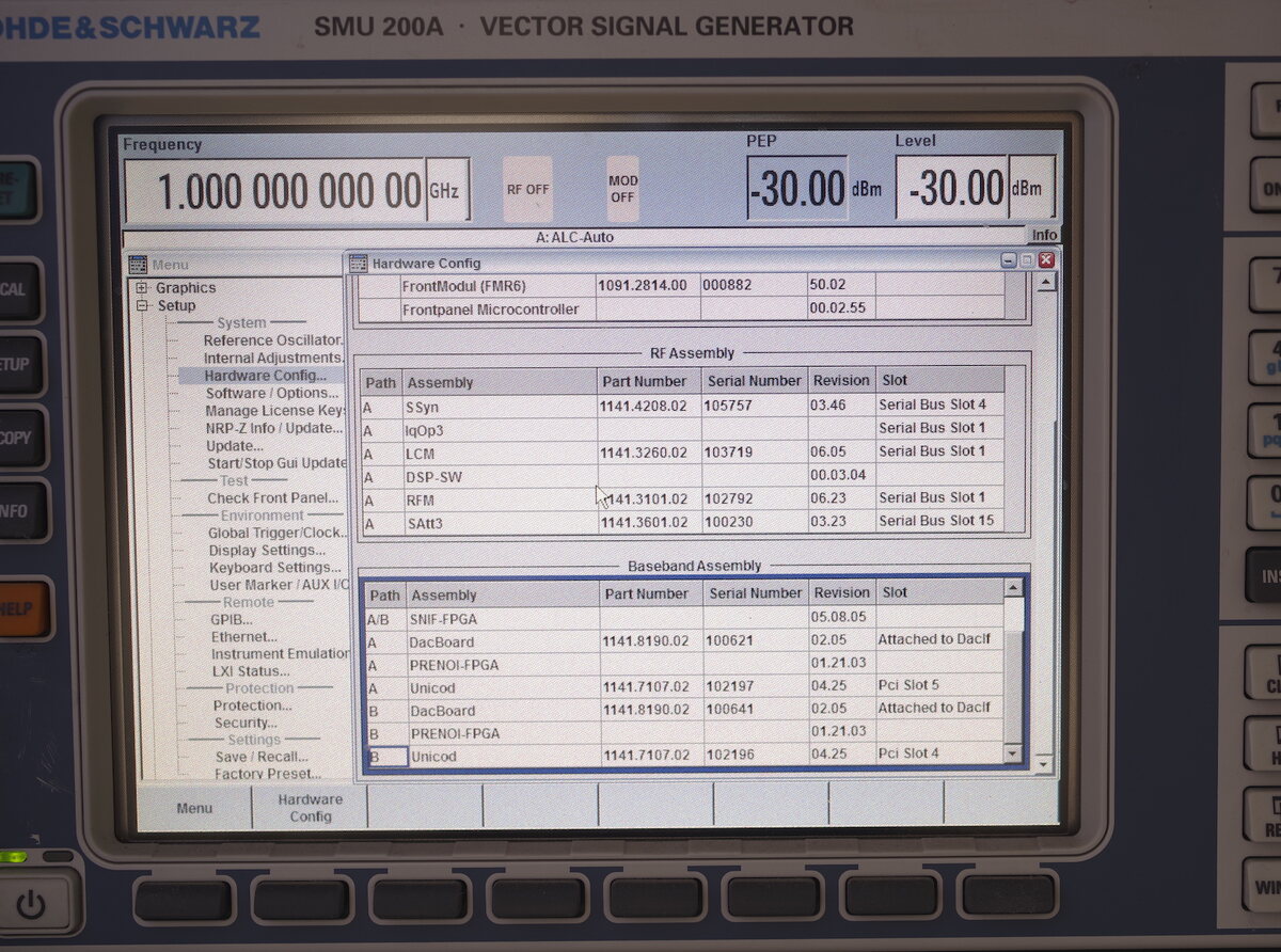
Display eines SMU 200A Vector Signal Generators
1141.3601.02 100230 03.23 Serial Bus Slot 15 Baseband Assembly A/B SNIF-FPGA 1141.8190.02 100621 05.08.05 Attached to DacIf Ethernet DacBoard 1141.8190.02 100641 01.21.03 A Unicod PRENOI-FPGA 1141.7107.02 102197 04.25 Pci Slot 5 B DacBoard 1141.8190.02 100641 02.05 Attached to DacIf B PRENOI-FPGA 1141.7107.02
in „[V] R&S SMU 200A Vektor Signal Generator“ · Markt · · Fotos
-
PDF
GD32F103xx_Datasheet_V2.5.pdf
- 20.00 - E - 9.00 - - 12.00 - - 16.00 - - 22.00 - E1 - 7.00 - - 10.00 - - 14.00 - - 20.00 - R1 0.08 - - 0.08 - - 0.08 - - 0.08 - - R2 0.08 - 0.20 0.08 - 0.20 0.08 - 0.20 0.08 - 0.20 θ 0° 3.5° 7° 0° 3.5° 7° 0° 3.5° 7° 0° 3.5° 7° θ1 0° - - 0° - - 0° - - 0° - - θ2 11° 12° 13° 11° 12° 13° 11° 12° 13° 11
in „Unterschiede CS32F103C8T6 und STM32F103C8T6“ · Mikrocontroller und Digitale Elektronik ·
-
PDF
schematics.pdf
CAS CKE SCKE 18 38 18 38 SRAS RAS CLK SCLK SRAS RAS CLK SCLK D5 1 U22 RESET 4 H7 2 BYTE SW6 SN74LVC1G08 U49 C4 39 39 11 N 8 SOT23-5 1 RY/BY~ ABE0 DQM 1 2 3 4 5 6 7 DQM 1 2 3 4 5 6 7 AMS0 4 H2 ABE1 N N N N N N N N N N N N N N AMS1 22 7 2 CE G G G G G G G G G G G G G G U39 SN74LVC1G08 J2OE MT48LC32M8A2 6
in „Versorgung“ · Digitale Signalverarbeitung / DSP / Machine Learning ·
-
PDF
ADIS16250_16255.pdf
auto-null and factory reset commands. provides a calibration range of 0 to 1.9995, and its contents The DAC latch command loads the contents of AUX_DAC into the are also nonvolatile. DAC latches. Since the AUX_DACcontentsmustbeupdated one byte at a time, this command ensures a stable DAC output voltage Table
in „Bias bei Gyro“ · Mikrocontroller und Digitale Elektronik ·
-
Datei
stm32f4_discovery_audio_codec.c
); /* Set the Master volume */ Codec_VolumeCtrl(Volume); if (CurrAudioInterface == AUDIO_INTERFACE_DAC) { /* Enable the PassThrough on AIN1A and AIN1B */ counter += Codec_WriteRegister(0x08, 0x01); counter += Codec_WriteRegister(0x09, 0x01); /* Route the analog input to the HP line */ counter += Codec_WriteRegister
in „STM32F4 Discovery Audio DAC CS43L22“ · Mikrocontroller und Digitale Elektronik ·
-
PDF
LGT8F328P.pdf
LGT8FX8P Series - Programming Manual 1.0.1 LogicGreen Technologies Co., LTD Digital-to-analog converter (DAC) https://translate.googleusercontent.com/translate_f 202/227 30/08/2017 LGT8F88P LGT8F168P LGT8F328P ● 8-bit digital-to-analog conversion output ● The DAC output can be used as an analog comparator
in „Neue 8-Bit Tinys vorgestellt: 417/814/816/817“ · Mikrocontroller und Digitale Elektronik ·
-
Datei
stm32f4xx.h
t RESERVED1; /*!< Reserved, 0x06 */ __IO uint32_t CR; /*!< CRC Control register, Address offset: 0x08 */ } CRC_TypeDef; /** * @brief Digital to Analog Converter */ typedef struct { __IO uint32_t CR; /*!< DAC control register, Address offset: 0x00 */ __IO uint32_t SWTRIGR; /*!< DAC software trigger register, Address offset: 0x04 */ __IO uint32_t DHR12R1; /*!< DAC channel1 12-bit right-aligned data holding register, Address offset: 0x08 */ __IO uint32_t DHR12L1; /*!< DAC channel1 12-bit left aligned data holding register, Address offset: 0x0C */ __IO uint32_t
in „STM32F0 Discovery und UART1“ · Mikrocontroller und Digitale Elektronik ·
-
Datei
stm32f4xx.h
t RESERVED1; /*!< Reserved, 0x06 */ __IO uint32_t CR; /*!< CRC Control register, Address offset: 0x08 */ } CRC_TypeDef; /** * @brief Digital to Analog Converter */ typedef struct { __IO uint32_t CR; /*!< DAC control register, Address offset: 0x00 */ __IO uint32_t SWTRIGR; /*!< DAC software trigger register, Address offset: 0x04 */ __IO uint32_t DHR12R1; /*!< DAC channel1 12-bit right-aligned data holding register, Address offset: 0x08 */ __IO uint32_t DHR12L1; /*!< DAC channel1 12-bit left aligned data holding register, Address offset: 0x0C */ __IO uint32_t
in „STM32F4 SPI Problem“ · Mikrocontroller und Digitale Elektronik ·
-
PDF
AD9857.pdf
s). 48, 54, 58, 64 36, 39, 40, 42, AGND Analog Ground pin(s). 44, 47, 53, 56, 59, 61, 65 45 IOUT O DAC Output pin. Normal DAC output current (analog). 46 IOUT O DAC Complementary Output pin. Complementary DAC output current (analog). 49 DAC_BP DAC Reference Bypass. Typically not used. 50 DAC_RSET I DAC
in „Updatepin zur Aktivierung beschriebener Kontrollregister“ · Mikrocontroller und Digitale Elektronik ·
-
PDF
AD9857.pdf
s). 48, 54, 58, 64 36, 39, 40, 42, AGND Analog Ground pin(s). 44, 47, 53, 56, 59, 61, 65 45 IOUT O DAC Output pin. Normal DAC output current (analog). 46 IOUT O DAC Complementary Output pin. Complementary DAC output current (analog). 49 DAC_BP DAC Reference Bypass. Typically not used. 50 DAC_RSET I DAC
in „Mit MSP430F2013 parallele Datenübertragung programmieren“ · Mikrocontroller und Digitale Elektronik ·
-
Datei
hardware_t.cpp
_2_bak = CH2_DAC_Correction_2; CH2_DAC_Correction_3_bak = CH2_DAC_Correction_3; CH3_DAC_Correction_1_bak = CH3_DAC_Correction_1; CH3_DAC_Correction_2_bak = CH3_DAC_Correction_2; CH3_DAC_Correction_3_bak = CH3_DAC_Correction
in „Wittig(welec) DSO W20xxA Open Source Firmware (Teil3)“ · Mikrocontroller und Digitale Elektronik ·
-
Datei
mispav.htm
=F 0.000000 7:1227=0x4CB=F 0.000000<br> qqmodbio:<br> r 2024-08-16 14:09:34.375Lese von 's'Slave=20 'a'Wortadresse=6 'n'Anzahl=2<br> modbus_read_reg() rva=12000<br> qqcrc16<br> FEHLER<br> <br> qqmodbio:<br> r 2024-08-16 14:09:40.656Lese von 's'Slave=20&
in „Implementierung von Menüs auf alphanumerischen Displays“ · Mikrocontroller und Digitale Elektronik ·