▯ } I ( ▯ 2 › 2 LED Driver IC ▯ D O ▯ î C ▯ +12V_FAN LED Forward Voltage E 2 2 1 1 SDICS ▯ +15V R_Max 2.4V x 4 pcs = 9.6V L L L L SDI_CLKL ) For EMI ▯ 3 3 3 2 2 2 1 1 1 G_Max 3.3V x 4 pcs = 13.2V C227 C100p50N0402 LED1_G L L L L L L L L L Pin Definerd 6 5 4 3 2 1 O ▯ C567 C100p50N04N2 LED1_R B_Max 3.3V
) Alarm: Once alarm/Everyday alarm:One system each FM S/N ratio: Monaura:l 70dB Sleep: Sleep timer:Max. 90 minutes Stereo:70dB n nGeneral FM THD+N (1kHz) :Monaura: l 0.4% Stereo:0.4% Power supply: (for E2): AC 230 V, 50 Hz / 60Hz (for E1C): AC 220V, 50Hz (for JP): AC 100V, 50/60Hz Power consumption:
percent (€12 million to €30 million) since Unabiz took charge in 2022 – it claims. Its total debt was €153 million in 2022, when the court-managed receivership process was to find a buyer; its debt is less than €5 million today, mostly inherited from long-term rental fees to French tower firms to stand-up
life. Moreover, the TLR1901GXZ features an exceptionally low input offset voltage of just 0.55mV (max.), one of the best among ultra-low current op amps. This represents an approximate 45% reduction compared to typical products on the market. A maximum input offset voltage temperature drift of 7µV/°
2025 6) ABSOLUTE MAXIMUM RATINGS All Voltages with Respect to Ground Parameter Symbol Conditions Min Max Unit Supply Voltage VDDV SS - 0.3 +6 V Input Voltage VIN VSS0.3 VDD0.3 V (1) ESD Rating VHBM Human Body Model (HBM) ±2 kV VCDM Charged Device Model (2) ±1 kV Latchup Current Limit LUT For all pins ±
edgemore) after the reference clock edge arrives arrives at the pin? at the pin? CLOCK_TO_OUT ALLPORTS MAX 10ns CLOCK_TO_OUT ALLPORTS MAX 10ns MIN 2ns CLKPORT “clk”; MIN 2ns CLKPORT “clk”; TRACE uses different performance grades and conditions when doing Setup time vs. Hold time analysis. Table 2 has more
Mittelwellenband randvoll ist mit Spaniern und massenhaft USA Stationen im 10 kHz Raster, die nur mit max. 50 kW senden dürfen, ist Grigoriopol geradezu ein Ortssender.
und keiner war an seiner Position auf der Skala zu empfangen. Und auf LW war besonders wenig los (max 4 Sender). Anbei mal der Beethoven 2 von 1956.
der Distribution upgradet (neben anderen Altlasten). Da reden wir aber über Größenordnungen von max. 10GB; eher *deutlich* weniger...geradezu lächerlich bei den aktuellen Massenspeichern, und ab und an ist es sogar recht nützlich auch die alten Library-Versionen zur Verfügung zu haben. Fazit: ausser
: 74h Size: 8 bits Table 3-213 Lock Count Bit Access Symbol Description [7:4] R/W locked_cnt_noisy_max These bits set the max value of the hlock sensor for noisy signals. 8 is added to this value. Default = 7 stands for 15. These bits set the max value of the hlock sensor for clean signals. 8 is [3:0] R/W locked_cnt_clean_max added to this value. Default = 4 stands for 12. 3.9.18 H Loop Max State Address Offset: 17h Access: Read/Write Default Value: CBh Size: 8 bits 83 电子专业技术主页: HTTP://WWW.LCDHOME.NET 资料收藏: 版权归原作者所有 谨供学习用
WITH −T− SEATING REFERENCED TO−204AA OUTLINE SHALL APPLY. PLANE E INCHES MILLIMETERS D 2 PL K DIM MIN MAX MIN MAX 0.13 (0.005) M T Q M Y M A 1.550 REF 39.37 REF B −−− 1.050 −−− 26.67 C 0.250 0.335 6.35 8.51 U D 0.038 0.043 0.97 1.09 −Y− E 0.055 0.070 1.40 1.77 V L G 0.430 BSC 10.92 BSC H 0.215 BSC 5.46
DIMENSION: INCH. 3. D DIMENSION SHALL BE MEASURED WITHIN D B DIMENSION P. INCHES MILLIMETERS DIM MIN MAX MIN MAX A 0.260 0.280 6.60 7.11 B 0.220 0.240 5.59 6.10 C 0.075 0.095 1.90 2.41 D 0.115 0.121 2.92 3.07 H 0.0020 0.0060 0.051 0.152 J 0.006 0.012 0.15 0.30 K 0.030 0.050 0.76 1.27 C P 0.020 REF 0.51
berechnen Sicherheitsabstände und Überspannungsschutz, durchaus Vpeak sinnvoll sein. iinput inrush,max (8) Rin In unserer Schaltung haben wir 300 Ω mit bedrahteten Der Vorwiderstand verursacht jedoch zu jeder Zeit während Widerständen realisiert, und der Einschaltstrom ist im des Wandlerbetriebs eine
temperature, R ILIM= 400 Ω, unless otherwise noted. TPS2112A TPS2113A PARAMETER TEST CONDITIONS MIN TYP MAX MIN TYP MAX UNIT VI(IN1)VI(IN2)5.0 V 120 140 84 110 T J 25°C, IL= 500 mA VI(IN1)VI(IN2)3.3 V 120 140 84 110 mΩ Drain-source V = V = 2.8 V 120 140 84 110 on-state rDS(on)) I(IN1) I(IN2) resistance VI
5.5 V, and RILIM 400 Ω, unless otherwise noted. TPS2114A TPS2115A PARAMETER TEST CONDITIONS MIN TYP MAX MIN TYP MAX UNIT T J 25°C, L = 500 mA, I(IN1)VI(IN2)5.0 V 120 140 84 110 mΩ T = 25°C, I = 500 mA, V = V = 3.3 V 120 140 84 110 mΩ J L I(IN1) I(IN2) Drain-source on-state T J 25°C, L = 500 mA, I(IN1)
20 A1, Frequenz- Smart PLGS 2012 A1. leistung.......≤20dBm Frequenzband ..2400-2483,5MHz Temperatur.max 50 °C Ladevorgang 0 - 10 °C, bzw. 50 - 60 °C bei einem Ladestrom von max. 4 A 10 - 50 °C bei einem Ladestrom von max. 12 A Betrieb......-20 - 50 °C Lagerung 8 DE AT CH Ladezeit Akku Smart PAPS 208 A1
erster Treffer von Google: https://elektro.turanis.de/html/prj153/index.html
Anhang. Beispielhaft die Kurven für 500mA (grün) und 1,2A (blau). Die Ausgangsspannung ist bei 500mA max. 6V (braun) und bei 1,2A max. 5,5V (violett). Der max. Strom wird mit dem 30R-Widerstand eingestellt, der genaue Wertebereich hängt vor allem vom Idss des JFet (BF256, BF244 o.ä.) ab.
constitutive equations - Part I: Rules developed with internal variables. J. Press. Vess. Techn. 105, 153-158. D.C. Drucker [1949: Relation of experiments to mathematical theories of plasticity. J. Appl. Mech. 16, 349-357. D.C. Drucker [1950: Some implications of work hardening and ideal plasticity. Quart
funktional. In dem Fall zwei Buttons mit Post-Methode ("Drehe links"/"Drehe rechts"). Auch das ist mit max. 50 Zeilen HTML+JS abgetan. Wer so etwas schon öfter gemacht hat und vielleicht schon auf vorhandene Codesippets zurückgreifen kann, wird vermutlich keinen halben Tag brauchen. Du mußt und willst
außer der typischen Beleidigung, > > Fragen Sie doch einfach Ihren Rechtsanwalt, ob er Ihnen die §§ 153 ff. > STPO und § 374 STPO erläutern kann. > >> Also... ich sage es mal so... als letzte Erklärung zu dem Thema, so daß >> vielleicht sogar Du es endlich verstehst. Es gibt hier in diesem Forum
place.The compressors will withstand storage temperatures down to -35°C. Condensing temperatures: Max. 60°C at stable conditions and max. 70°C at peak load. Ambient temperatures: Min. -10°C, max. 55°C The BD compressor concept includes an electronic unit which features overload protection, battery protection
generated when the counter is equal to TOP. If TOP is updated to a value lower than count upon reaching MAX the counter restarts from BOTTOM. Figure 21-3. Periodic Interrupt Mode MAX and Event) Request TOP CNT BOTTOM TOP changed to CNT set to BOTTOM a value lower than CNT 21.3.3.1.2 Time-Out Check Mode In
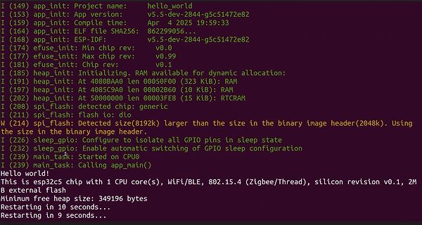
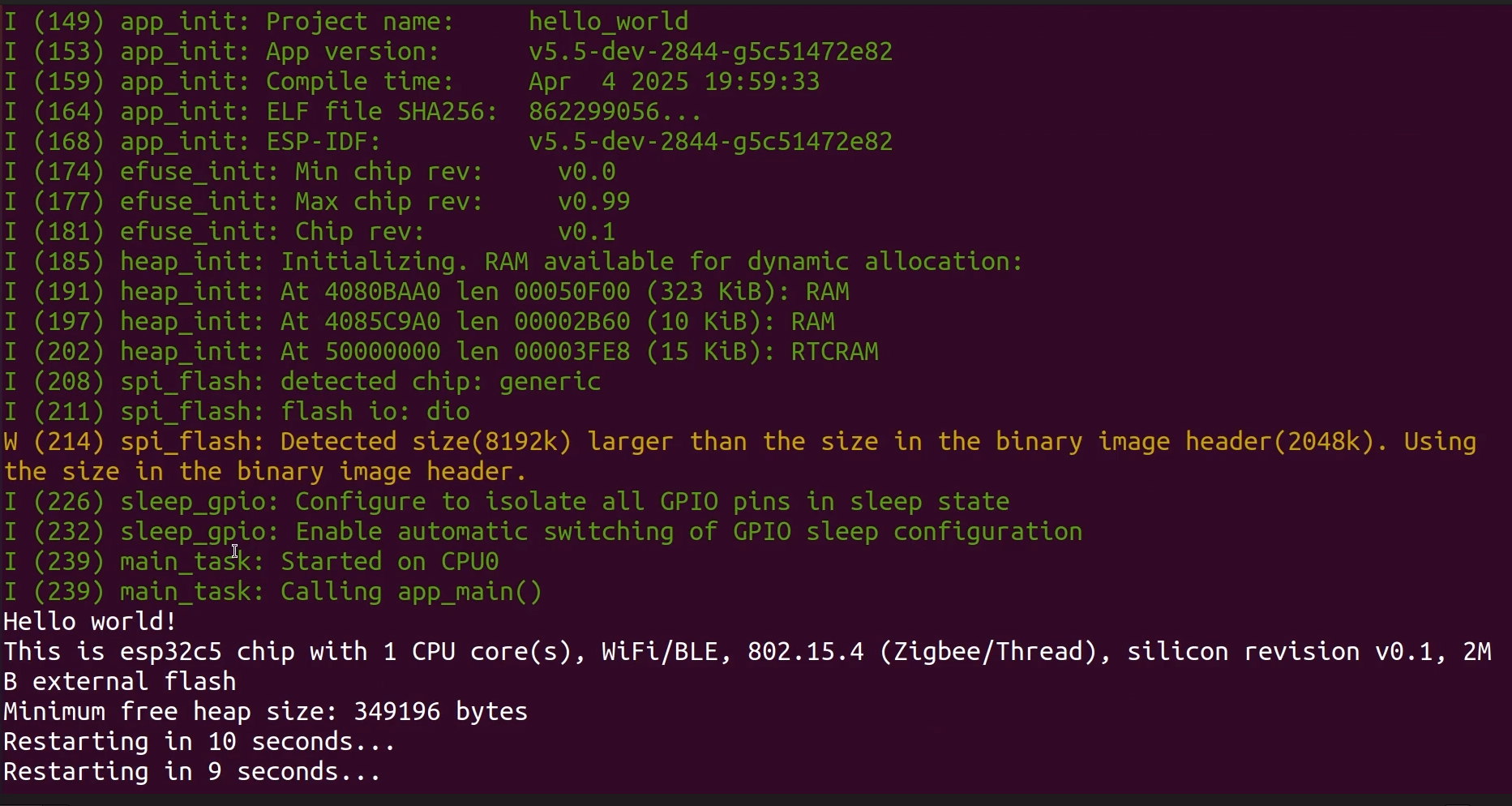
I (149) app_init: Project name: hello_world
I (153) app_init: App version: v5.5-dev-2844-g5c51472e82
I (164) app_init: Compile time: Apr 4 2025 19:59:33
I (168) app_init: ELF file SHA256: 862299056...
I (174) app_init: ESP-IDF: v5.5-dev-2844-g5c51472e82
I (177) efuse_init: Min chip rev: v0.0
I (181) efuse_init: Max chip rev: v0.99
I (185) efuse_init: Chip rev: v0.1
I (191) heap_init: Initializing: RAM available for dynamic allocation:
I (197) heap_init: At 4080BA0 len 00050F00 (323 KiB): RAM
I (202) heap_init:
Symbol Parameter Conditions Tamb = 25 °C T amb = -40 °C Tamb = -40 °C Unit to +85 °C to +125 °C Min Typ Max Min Max Min Max 74HC138 VIH HIGH-level VCC = 2.0 V 1.5 1.2 - 1.5 - 1.5 - V input voltage V = 4.5 V 3.15 2.4 - 3.15 - 3.15 - V CC VCC = 6.0 V 4.2 3.2 - 4.2 - 4.2 - V VIL LOW-level VCC = 2.0 V - 0.8 0.5
Voltages are referenced to GND (ground = 0 V) Symbol Parameter Conditions 74HC74 74HCT74 Unit Min Typ Max Min Typ Max V supply voltage 2.0 5.0 6.0 4.5 5.0 5.5 V CC VI input voltage 0 - V CC 0 - V CC V VO output voltage 0 - V CC 0 - V CC V Tamb ambient temperature -40 +25 +125 -40 +25 +125 °C Δt/ΔV input
(ground = 0 V). Symbol Parameter Conditions 25 °C -40 °C to -40 °C to Unit +85 °C +125 °C Min Typ Max Min Max Min Max 74HC08 V HIGH-level V = 2.0 V 1.5 1.2 - 1.5 - 1.5 - V IH CC input voltage VCC = 4.5 V 3.15 2.4 - 3.15 - 3.15 - V VCC = 6.0 V 4.2 3.2 - 4.2 - 4.2 - V VIL LOW-level VCC = 2.0 V - 0.8 0.5
MAN’X TOP AMM/DMM ISO 72,39 6101 Chauvin Arnoux MAN’X TOP PLUS AMM/DMM ISO 72,39 6102 Chauvin Arnoux MAX 1000 AMM/DMM ISO 72,39 6103 Chauvin Arnoux MAX 2000 AMM/DMM ISO 72,39 6104 Chauvin Arnoux MAX 3000 AMM/DMM ISO 72,39 6105 Chauvin Arnoux MC 5 B Prüfspannungsgenerator ISO 88,08 6106 Chauvin Arnoux MN89
Characteristics. ............5 • Changed V FBTH - T A –40°C to 85°C, V = 1.05 VO continuous mode From: MIN = 751 MAX = 779 mV To: MIN = 754 MAX = 776 mV in the Electrical Characteristics................................................................................5 • Changed the Over/Under Voltage Protection section
sentido horário, [MULTICHANNELDECODING],SOUNDFIELD[2CH],SOUND “VOL MIN”, “VOL 1” para “VOL 30”, “VOL MAX” aparecem. CONTROL [SURR] e [NAME] LED acendem. 4. Pressione a tecla [VIDEO 1] , todos os seguimentos apagarão. 5. Toda vez que pressionar a tecla [VIDEO 1] um conjunto de seguimento e LED acenderá
REF = 4.096 V (internal), SDO load = 20 pF, and f SAMPLE = 500 kSPS, unless otherwise noted. MIN TYP MAX UNIT TIMING SPECIFICATIONS fS Sampling frequency (f CLK = max) 500 kSPS tS ADC cycle time period (f CLK = max) 2 µs fSCLK Serial clock frequency (f S max) 17 MHz tSCLK Serial clock time period (fS=
Max G. schrieb im Beitrag #7815461: > Ich finde die Dinger bei Amazon zu relativ erträglichem Tarif: > https://www.amazon.com/CS830-CS830A4RD-Brand-Original-Power/dp/B09KM1FG5D Aber die Lieferzeit.
. Der IC ist nach Datenblatt stabil. Die Folienkondensatoren an der Drossel (MKP62 474M / MMKP82 153J1000 (J Kondensatoren müssen wohl verboten sein auf dem Markt als Ersatzteil ..😡)) sind ziemlich an der Grenze - aber unmöglich zu beschaffen. So wie die meisten Teile, die kaputt gehen. Da muss ich
Vb 1 7867 o t a l t ED ED ED s n I a b ED ED Va Vb a b ED ED Va Vb a b ED ED Va Vb 1 7867 ED ED ED max. 30 max. 30 max. 30 L N Va Vb L N Va Vb L N Va Vb 1 6481 L N 1 2 3 4 11 21 a1 b a2 b a3 b 1 7573 Va Vb Va Vb + E+ Va Vb Va Vb 1 4813 1 8783/ Va Vb 80 1 2 1 8789 LT 1 2 3 4 1 8759/ 1 8760 1 8753 S0251
Characteristics V CC = 4.5V to 5.5V unless otherwise specified h r o a Symbol Parameter Conditions Min Max Units n l I Operating Current CS = V , SK=1.0 MHz 1 mA o C CCA IH u M ICCS Standby Current CS = V IL 50 µA s O B S IIL Input Leakage V IN0V to V CC ±-1 µA u E OL Output Leakage (Note 2) ) E P VIL Input
SSB Adjust the correct x, y coordinates (while holding one of the White point registers R, G or B on max. value) by means of 6.1 General Alignment Conditions decreasing the value of one or two other white points to the Perform all electrical adjustments under the following correct x, y coordinates (see
differential pair, the transducer's layout used a cross-quad geometry. Variations in process parameter A .v max(A),max(B) min(A),max(B) Variations 1/2 of device 1 1/2of device 2 in process . parameter B l _ II _ max(A),min(B) min(A),min(B) F 1/2 of device 2 1/2 of device 1 Figure 3.15: Cross-quad layout sketch
noted) (see Figure 16) STANDA2D MODE FAS2 MODE FAST MODE2PLUS (FM+) I C BUS I C BUS I C BUS UNIT MIN MAX MIN MAX MIN MAX scl I C clock frequency 0 100 0 400 0 1000 kHz sch I C clock high time 4 0.6 0.26 μs 2 scl I C clock low time 4.7 1.3 0.5 μs t I C spike time 50 50 50 ns sp sds I C serial data setup

 Bild
 Bild
 Bild
 Bild