Energizer Lithium korrelieren mit deren Datenblatt, sind also plausibel: http://data.energizer.com/pdfs/l92.pdf Wieviel Kapazität hast du bei den Varta Lithium AA gemessen und bei welchem Strom?
1 D D D D D D D D D N P P V V R R G G T T V W / / A A F / A A F / A R # # + X + X W E E X R T T P L L R O ED / E X S F Final 5 Version: DM9161-DS-F05 September 10, 2008 DM9161 10/100Mbps FastEthernetPhysicalLayer TX/FXSingleChipTransceiver 5. Pin Description I: Input, O: Output, LI: Latch input when
3 3 3 3 3 3 3 3 2 2 2 2 2 2 2 2 2 2 1 2 3 T H O +F F M H O - F T V 2 3 3 3 P C3 = 0.22µF S S S E F L E R O N L A U I G C A G B C4= 100pF O O O T R E CR C C I I B R C5 = 0.02µF R1= 24kΩ ICL7106 R = 47kΩ 4 L 2 + 1 1 1 1 1 1 1 2 2 2 2 2 2 3 3 3 3 B O R3= 100kΩ V D C B A F G E D C B A F E D B F E A P R4
8 1 S ST9 G SMD A1 R21 BC858 120 SMD D D D 12V 2A SMD +5V S S S ST10 D2 +5V Q1 1 IC6 3 R 7 R 7 R 7 78L05 IC2 D 4,194304 +5V 4 4 4 1N4001 1 A1 VCC 8 R 0 M 2 A2 Test 7 1 S 1 MHz 230V~ 2 3 A3 SCL 6 A A A A A C1 C2 C3 C4 C5 C6 50Hz C12 C13 C18 4 GND SDA 5 T T T T T x2401 SMD + - 22p 22p 470n 100n 100V 100V 220u 100n 10u T1 T2 T3 SMD SMD SMD SMD 40V SMD 25V EEPROM S 8 4 1 M -5V D LS L D3 IC7 R11 79L05 120k 1N4001 C7 C17 C19 IC3 SMD/1% -5V C10 47u 100n 10u +5V 330p IC4 +5V 25V SMD 25V 2 - SMD 1 7 VEE C 9 4 A + IC3 % 4 7 B 10 IC3 D k 3 + 5 0 / 2 6 A 11 5 k D 8 M 8 1 6 R 3 M 5 5 R 1
Martin L. schrieb im Beitrag #7986953: > Den gelben Kondendator (links oben im Bild 5777), genau da, wo du deinen > Finger hast, der könnte ein Kandidat sein. Die unten links? Die sind nur für den up/down
eines für die Display-Platine (beide durch Optokoppler getrennt). Der obere Strang für über einen 78L05, der untere hat den Spannungsregler wohl auf der Displayplatine, da ist nur eine einfache Didoe zur Gleichrichtung und ein kleiner Elko zur Glättung angebracht.
and linearity. 3. Make the following display monitor adjustments as determined in step 1. a. Adjust L4 (WIDTH) so that the width of the Analyzer display at the center is 5.04 inches (12.80 cm). b. Adjust R43 (V SIZE) so that the height of the Analyzer display at the center is 3.78 inches (9.60 cm). c
device which is to be protected. For devices such as the PAC DN004, 6, or 7 this is Vcc Vcc Parasitic L ESD Entry Parasitic L PDeviceed Point Deviceted ESDEntryPoint Gnd Gnd Bad layout - increased clamp voltage due Preferred Layout to parasitic inductance Figure 10: The Need to Keep ESD Diodes Downstream
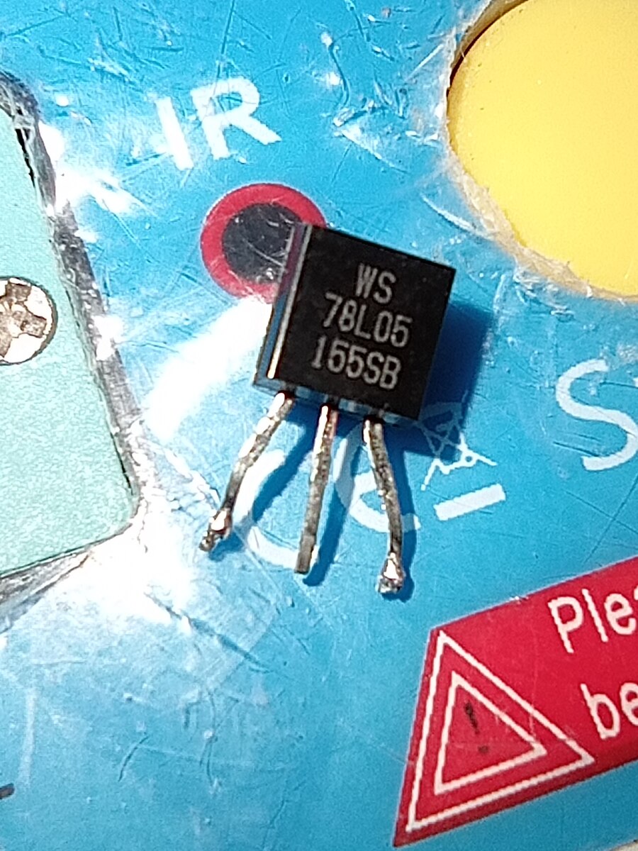
Hallo Leute, eine interessante Beobachtung zum T7 Mini-Tester: Wenn man z. B. einen 78L05-Spannungsregler einsetzt, wird er vom Tester oft als Transistor erkannt, mit einem hFE < 1. Das liegt am Algorithmus der Firmware, nicht an einem Defekt des Bauteils. Daran sieht man, dass 3-beinige
Bit_72 bit 0x72 Bit_73 bit 0x73 Bit_74 bit 0x74 Bit_75 bit 0x75 Bit_76 bit 0x76 Bit_77 bit 0x77 Bit_78 bit 0x78 Bit_79 bit 0x79 Bit_7A bit 0x7A Bit_7B bit 0x7B Bit_7C bit 0x7C Bit_7D bit 0x7D Bit_7E bit 0x7E Bit_7F bit 0x7F P00 bit 0x80 P01 bit 0x81 P02 bit 0x82 P03 bit 0x83 P04 bit 0x84 P05 bit 0x85
DB 0xD2 ;D2 -- '' DB 0x37 ;37 -- '7' DB 0x20 ;20 -- ' ' DB 0xB3 ;B3 -- '' DB 0x2A ;2A -- '*' DB 0x05 ;05 -- '' DB 0x4C ;4C -- 'L' DB 0xE5 ;E5 -- '' DB 0x4C ;4C -- 'L' DB 0xB4 ;B4 -- '' DB 0x0A ;0A -- '' DB 0x00 ;00 -- '' DB 0x40 ;40 -- '@' DB 0x21 ;21 -- '!' DB 0x75 ;75 -- 'u' DB 0x4C ;4C -- 'L' DB
USB_P4 42_CHARGER ENE UB6225P PCIE_2 43_VCORE(7A) Card Reader LAN RJ-45 44_POWER_3V_5V_VTT_DDR Attansic L2 USB_P7 45_POWER_3VA_3VSB Camera 46_POWER_1.05V_1.5V_2.5V Onboard 47_POWER_1.8V_DUAL_5VSB USB_P0 IDE Master Flash Controller SM223 NAND Flash SATA1 A NAND Flash Flash Conn A Card IDE Slave <Variant Name
Temperature Min (T s(min) 150°C Ramp-up Critical Zone TLtoPT Pre Heat -Temperature Max (T s(max) 200°C L tL T -Time (min to max) (s ) 60 – 180 secs es(max) t Average ramp up rate (LiquidusTemp (T )A e Ramp-down 3°C/second max ps(min) to peak e Preheat T T S(max)T A Ramp-up Rate 3°C/second max -Temperature
can be calculated from Equations 12 and 13: 2 VDD CSNUB = - - - - -2- - RSNUB = - - - - 2F ring L CSNUB RAMP GEN V RAMP= VDD/11 (EQ. 12) (EQ. 13) L R Input Capacitor Selection - E + I The input capacitor absorbs the ripple current from the D CO synchronous buck converter, which is given by Equation
nRESET/PA7 4 7 PA1/ADC1/PWM1O/INT1/PSCL PWM0N/ADC6/PA6 5 6 PB0/ADC7 DS-TM56M152A_E 12 Rev 0.96, 2024/05/16 TM56M152A Data Sheet TM56M152A L S / T T D N N S / / / 2 1 5 M M M W W W 3 1 0/ C C C A A A S 3 1 0/ V P P P 1 1 1 1 VCC 1 12 PA2/ADC2/PWM4O/TM0CKI PWM0P/ADC4/PA4 2 11 PB6/ADC12 PWM3O/ADC5/PA5 3 QFN
Sheet PIN SUMMARY Pin Number GPIO Alternate Function 0 6 4 ) 0 Input Output - - - -P - O 0 O O O F l r l s o ( - ( ( ( ( p t n p n P i a 2 P 2 2 2 2 Pin Name y o o r u r s 2 M C a S 4 S 4 4 6 4 T C n t e D u ( P A p M E T E E E E p w I a e S C o 5 ( 5 5 5 5 l - t W p O V C M M M M M u l E O M / T T
Switching Non-shorting Electrical Characteristics Distance Between Horizontal Min.: 12.7 (0.500) or 17.78 (0.700) Switiching Power Max. 240 mW DC Button Centers Vertical Min. 17.78 (0.700) SwitchingVoltage Max. 24 V DC Terminals PC pins Switching Current Max. 10 mA DC Mounting Soldering, centering pins Carrying
±0.05 2.25±0.05 4 3 2 1 5 6 78 Feed direction No. PH008-A-C-SD-2.0 TITLE SNT-8A-A-Carrier Tape No. PH008-A-C-SD-2.0 ANGLE UNIT mm ABLIC Inc. +1.0 9.0- 0.0 11.4±1.0 Enlarged drawing in the central part ø13±
power delivered to the load and the available power of the source. 2 2 2 |S21 ·(1 − |r S )·(1 − |r L ) G T |1 − r ·S − r ·S + ∆·r ·r | 2 (4.77) S 11 L 22 S L The transducer power gain can be split into three parts [6]: G T G ·G SG 0 L (4.78) with (1 − |S | )·(1 − |r1| ) G S (4.79) |1 − rS·r 12 2 G 0
network To VR_PA VR_PA filtering and biasing (C 9, C10, 6) C9 C 10 Band-stop to filter the 2dharmonic (L 2,C 2 C2 L6 DC block capacitor (C 4) To RFO_HP DC block capacitor (C 6) Connector L1 L2 C 4 L3 CTRL or or RFO_LP C 6 L 4 PCB antenna (PA output) C5 C1 C 3 RF or antenna switch C 7 C8 L-C matching C-L-C
Characteristic Curves 100 1.E-03 t =0.4 ms T = 235 °C J 1.E-04 10 TJ= 200 °C T = 235 °C ) ) J ( 1.E-05 ( IR TJ= 150 °C IF t t 1 r 1.E-06 e T J 200 °C u TJ= 100 °C u C C g r 0.1 T J 150 °C a 1.E-07 T J 60 °C a a r L F T J 100 °C s 1.E-08 e 0.01 e T J 25 °C T J 60 °C R 1.E-09 T J 25 °C 0.001 1.E-10 0.0
PD-96231 IRLB8748PbF HEXFET Power MOSFET Applications l Optimized for UPS/Inverter Applications V DSS R DS(on) max Qg l High Frequency Synchronous Buck 30V 4.8m : 15nC Converters for Computer Processor Power l High Frequency Isolated DC-DC D Converters with
CRC register one bit to the right (toward the LSB), zero–filling the MSB. Extract and examine the L.B 4. (If the LS was 0): Repeat S tep 3 (another shift). (If the LSB was 1): Exclusive OR the CRC register with the polynomial value 0xA001 (1010 0000 0000 0001). 5. R epeat Steps 3 and 4 until 8 shifts
3.3V Regler Die aufgedruckten Bezeichnungen sind meistens klar, ein "HT7133" enthält die 3,3V und 78L05 sollte ein 5V-Regler sein. Aber ein Foto des Moduls brächte noch mehr Klarheit, und wir könnten nachfragen.
) 78 /H/P_ON PU O O/L O/L O/L O/L O/L TAS 5558 Headphone in/out selector (12 pin) 79 /5558_PDN PU(DTA) O O/L O/L O/L O/L O/L TAS 5558 Power down (12 pin) 80 /5558_MUTE PU(DTA) O O/L O/L O/L O/L O/L TAS 5558
Markus L. schrieb im Beitrag #7938041: > Googel doch. Frechheit!
1,5 A Dauerstrom (?) liefern- Dann genügend Impulsbelastung haben. So mit 10000 µF Ladeelko und UA78H05 und Konsorten wäre schon etwas denkbar. Wie sieht es mit der minimalen Spannungsanstiegszeit aus? Viele µCs gehen direkt in den Broutout, wenn nicht innerhalb von 10 ms mindestens der Brounoutlevel
) V RANGE = ±1.5V TO ±5V B 3 B 0.3 VS = 20mV p-p ( ( OUT N 0 N 0.2 A A G –3 G 0.1 P 0pF P O –6 O 0 L L - –9 D–0.1 E 5pF E S –12 S–0.2 L L C –15 C–0.3 V RANGE = ±2.5V TO ±5V 10pF VS = 2V p-p –18 –0.4 OUT 15pF –21 –0.5 –24 –0.6 0 0.1 1 10 100 2 0.1 1 10 100 1000 1 1 FREQUENCY (MHz) 2 FREQUENCY (MHz) 1
100NK 100V P/E P5 C5 23620-0268 CAP 220NK400VP/E 468 SER P15 C31 25061-0201 LED - T1 R'ND(3mm) RED L/LEG LED1 25115-0700 DIO 11DQ03 D1 25117-0020 DIO 1N5401 D2-6 27160-0011 IC V/REG 78L05 TO92 IC5 43171-2700 CONN ASSY 10W 400 ST QL-T PJ2 43187-2010 WIRE SET CUT nQL AUX UL 2 PASSES OF EACH WIRE THROUGH L2 44117-0211 PCB ASS SM AUX TERM/POWER nQLT PCB ASSEMBLY – SM AUX TERM/POWER Part No. Description Position 22041-0100 BEAD FERRITE SM0603 FB1-2 22156-0070 CHOKE SM 33uH 4.2A SHIELDED L1 23105-1100 RES
these lines. Figure 2-1 shows a typical implementation of the I C physical layer. VDD SDA SCL D A L D A L D A L D A L D D C D D C D D C D D C V S S V S S V S S V S S Microprocessor Microprocessor Peripheral Controller 1 Controller 2 Target 1 Peripheral Target 2 D D D D G G G G GND GND Figure 2-1. Typical

 Bild

 Bild

 Bild