unlikely to cause harm. 0.01 - 0.1 J May cause a mild shock; usually not dangerous. 0.1 - 1 J Can cause pain; risk of injury increases. 1 - 10 J Potentially dangerous; can cause serious injury or death, especially if the current passes through vital organs. > 10 J Highly dangerous; can be lethal, especially at higher voltages. Fliegenklatsche: 0,025 mJ 0.00002475 J Ich würde mit dem Kondensator jedenfalls nicht spielen, auch wenn es nicht tödlich ist, Nervenschäden kann ich nicht gebrauchen. Das heimtückische
selected so that a broad range of lower order modes in the plate the partial with higher amplitude. This can be seen on Fig. 3, where can be promoted [23]. By controlling plate material properties, the fundamental frequency is plotted in gray. the modal density at low frequencies can be optimized. As in The
C1 is selected between 100uF-470uF. C. There is no restriction on the type of capacitor C1, which can be a ceramic capacitor or an electrolytic capacitor. The logic power supply VCCx to ground capacitor C2 must be at least 4.7uF. In actual application, there is no need to add a separate capacitor close
)\Atmel\Studio\7.0\shellutils;;%PATH% set vers_h=01 set vers_l=44 set name=PU-Module set mcu=90can128 set fcpu=16000000 :set fcpu=8000000 set lib1=../../Devices2020/ModuleInterface set lib2=../../ModuleInterface set lib3=../Lib set crcstart=0x2234 set main=%name%_V%vers_h%.%vers_l% REM
90-day basic DC voltage accuracy and 0.008% 90-day basic resistance accuracy. At 6½ digits, the multimeter delivers 50 triggered readings/sec over the IEEE-488 bus. At 4½ digits, it can read up to 2000
2.1 I2C Command Protocol Before your tester writes IC commands to T100, slave address must be set at 50h. The timing sequence can be shown as below. After 4 cycles, the tester can get started IIC commands. SDA(A3) can affect slave address. Set low for 40h. Set high for 50h. 2 Cycles 2 Cycles XTALI RSTB
timeout periods (Table 1). Timeout settings of 100ms. This output structure sinks current when WDO can be hard wired, or they can be controlled with logic is asserted. Connect a pullup resistor from WDO to any gates and modified during operation. To ensure smooth supply voltage up to +5.5V. transitions
The temperature of a lead terminal. TSP Temperature Solder Pad: The maximum solder temperature that can be safely applied to the terminal. V K Knee Voltage: A specified regulator voltage near the lower knee of the current-regulating characteristic. V L Limiting Voltage: The voltage at pointLI on the current-voltage
darüber, dass IAR vom Cross-Plattform-Spezialisten QT übernommen wird: [c] The cash deal, which at SEK180 is a 66% premium on the current share price. has the backing of the main institutional investors with 38% of the shares. Completion of the deal is conditional on 90% of the shareholders selling
work together to quickly shut off the PWM output when an overcurrent is detected. The shutdown state can be selected according to the inverter specifications. [/c] Das Gesamtportfolio präsentiert sich nun wie in der folgenden Abbildung gezeigt.  Bildquelle: https
Solderable • Maximum Lead Temperature for Soldering Purposes: 350°C 3/8″ from Case for 10 Seconds at 5 lbs. Tension • Polarity: Indicated by Diode Symbol or Cathode Band MR2535LAYYWW G G MAXIMUM RATINGS (TJ= 25°C unless otherwise noted) Rating Symbol Value Unit DC Peak Repetitive Reverse Voltage V 20
the routine after a programmed start time so that you can reprogram the start time. Display 91 TAKE FIRST SAMPLE AT HH:MM DD-MMM This display appears when you have selected “YES” in Display #90. Enter the start time and date for the flow -pulse countdown.
( R ( 3 7 ( 1 m 0 1 6 1 12 (2.4) 2.0 1.0 0.4 0.5 2.0 Specifications SANYO: SIP12H Maximum Ratings at Ta = 25°C Parameter Symbol Conditions Ratings Unit Maximum supply voltage VCC max No signal 24 V Maximum output current o peak Per channel 2.5 A Allowable power dissipation Pd max Infinite heat sink
IRLZ44NPBF uses advanced trench technology and design to provide excellDS(ON)ith low gate charge. It can be used in a wide variety of S applications. D G TO-220 General Features VDS=60V,ID=60A PIN2 D ! RDS(ON) 20mΩ @ VGS=10V " ! " PIN1 G " Application ! PIN3 S High efficiency switch mode power supplies
longevity charge operation 5 — Fast charging beyond 50 kW Power sharing delivers high utilization 90kW Charging Points Retail/Shopping Sites Highway corridors and Fleets Terra chargers can provide a The Terra 124 charger can The Terra 184 chargers can add quick refill adding 100 miles of provide a full
input, 3.7V/2A conversion ÿ Built-in power MOS The conversion efficiency is 94%; the charging current can be set through an external resistor. ÿ 750KHz switching frequency, can support 1uH inductor The input voltage of IP2312 is 5V, and the input can intelligently adjust charging. ÿ Input overvoltage and
T2 as the fulcrum stems from the fact that there cannot be a discontinuity in the transfer function at T2. The user can, however, set the DRC parameters to realize a discontinuity in the transfer function at the boundary defined by T1. If no discontinuity is desired at T1, the value for the offset term
particular our first multicore support! Initially available on the RP2040 microcontrollers, now TinyGo can use both cores at the same time for true concurrency in hardware. Another very powerful new capability added in this release is USB Mass Storage Device (MSD) support on the RP2040/RP2350, SAMD21, and
für den Standalone-Einsatz vorgesehene Arduino Stella, der zum Zeitpunkt der Drucklegung um rund € 90 den Besitzer wechselt. 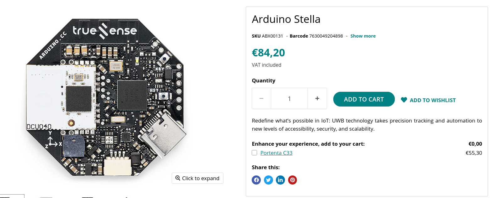 Bildquelle: https://store.arduino.cc/products/stella Als Funkmodul kommt hier ein DCU040 zum Einsatz. In der Pressemitteilung vermelden die
Hallo, ich möchte einen AT90CAN128 über die serielle Schnittstelle programmieren. Dafür suche ich einen geeigneten Bootloader. Im Internet habe ich "ATmegaBOOT_168_at90can.hex" und "AVR-CAN_UART.hex" gefunden und mit einem
Nachtrag Ich habe eine Olimex AVR-CAN-Platine. Wenn ich das Blink-Programm mit dem AVR-Prog herunterlade, erhalte ich folgendes: avrdude -F -V -c avrispmkII -p c128 -P usb -U flash:w:0_blink_can128.hex:i avrdude: AVR device initialized
Die zwei Adressen wurden auch hier beobachtet: https://docs.buspirate.com/docs/devices/at24c256/ " This AT24C256 EEPROM is a non-original variant and includes an additional address: 0x58 (0xB0/B1). This extra address can be utilized to store data, such as a serial number. While this feature is not supported in the official AT24C256 chip, it is commonly found in certain “AT24C256 boards” sold on platforms like AliExpress. Just use the 0x50 (0xA0/A1) address for reading and writing data to the EEPROM and ignore the 0x58 (0xB0
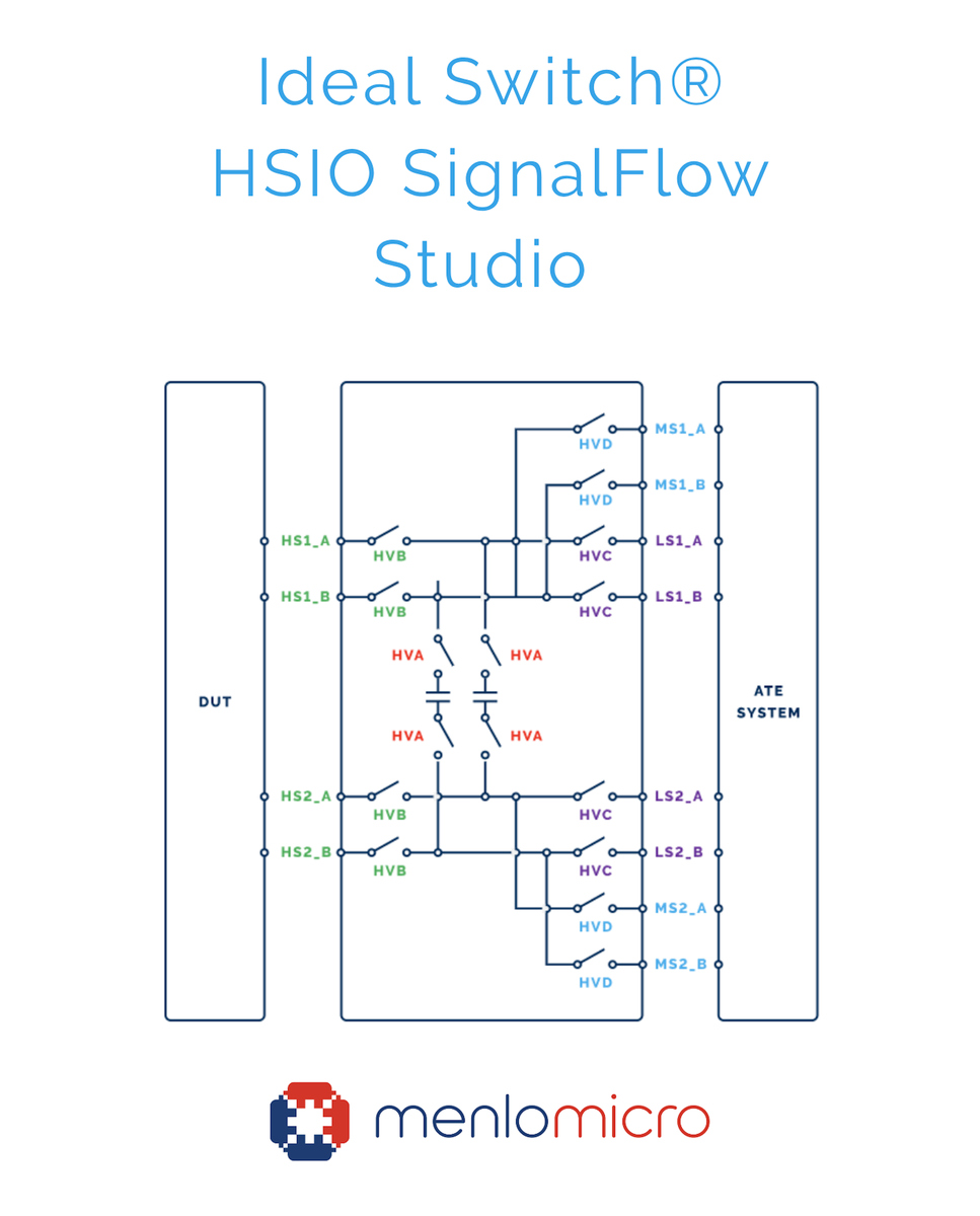 Bildquelle: Menlo Micro. ### STMicroelectronics HFDA80D / HFDA90D - Audioverstärker für den Automobilbereich. Wer einen Audioverstärker mit normalen Ansprüchen realisieren möchte, sollte heute so gut wie immer zu einem integrierten Schaltkreis greifen. ST schickt
● CPU load and task execution graphs ● Support for custom tracepoints Developers can use View for free, and registration unlocks additional features at no cost. [/c] ### ic-Haus iC-LFMB - neuer Linien-CCD ic-Haus ist einer der wenigen „rein deutschen“ Halbleiter-Hersteller: Das
definitions apply. Reading at any address within erase-suspended sec- tors produces status data on DQ7–DQ0. The system can use DQ7, or DQ6 and DQ2 together, to determine if a sector is actively erasing or is erase-suspended. Notes
current of just 250nA. They also offer an independent operating clock for the low-power UART, which can be used to wake up the system when receiving data from Wi-Fi and/or Bluetooth® LE modules. Along with the USB-C support, this combination of features makes the RA2L2 the premier solution available for
prices for the R2S as for the earlier RV and RV2 SBCs: • 2GB RAM – $30.00 • 4GB RAM – $39.90 • 8GB RAM – $49.90 (TBD) [/c] ### Meadow.Blazor integiert Meadow-APIs in Blazor-Applikationen Bryan Costanich’s Meadow-Ausführungsumgebung erlaubt die Nutzung von .net-Code zur Ansteuerung
parallel connected chips as e.g. the For investigating the switching behaviour of the Super CM400HB-90H for high currents are applied. In these large Cascode in detail, a half bridge with two switches consisting of modules, which usually are operated at relatively low switch- a MOSFET and 5 cascaded JFETs
will be (18 – 17.2) kHz = 0.8 kHz. L2/C2 is a bandpass filter, letting signals only with frequencies at and around 0.8 kHz pass. The 0.8 kHz signal then goes to the volume control P1, audio amplifier IC1 and the output jack J3.Also to J4, where a loudspeaker can be conncted. The output power, however,
/ output terminal and ground terminal. 7.6 Temperature Meet item 3. Capacitance shall be measured at each step specified Characteristics in Table 3 after reaching the thermal equilibrium. The capacitance change against the capacitance at step 3 shall be calculated. Table3 Step 1 2 3 4 5 Temp. +20±2
and there will be no data displayed on output pin at all. After the memory device completes embedded operation (automatic Erase or Program), it will automatically re- turn to the status of read array, and the device can read the data in any address in
centered in the visible spectrum (VIS), plus one near-infrared (NIR) and a clear channel. Applications can be assisted to allow classification of ambient light and an integrated flicker detection channel that can automatically flag ambient light flicker at 50/60 Hz as well as buffer data for externally
or equivalent Ein E o R C L 3.0 V 50% 50% C E in TLHand tTHL PLH measured 1/4 Response Node E 10% − 90% O V MC1489A VO tTLH in t THL 1.5 V 1.5 V C L 15 pF = total parasitic capacitance which includes C, capacitor is for noise filtering. probe and wiring capacitances R, resistor is for threshold shifting
-> =thread-group-added,id="i1" -> ~"GNU gdb (Arm GNU Toolchain 14.2.Rel1 (Build arm-14.52)) 15.2.90.20241130-git\n" -> ~"Copyright (C) 2024 Free Software Foundation, Inc.\n" -> ~"License GPLv3+: GNU GPL version 3 or later <http://gnu.org/licenses/gpl.html>\nThis is free software: you are free to
http://openocd.org/doc/doxygen/bugs.html CDLiveWatchSetup embedded:startup.tcl:28: Error: Can't find raspberrypi-swd.cfg in procedure 'script' at file "embedded:startup.tcl", line 28 [/code]
active at 1. In interrupt trigger mode, when THR empty interrupt from UART is received, if FIFO is enabled, up to 8 bytes can be written to THR and FIFO at a time, and then will be transmitted automatically by
should match the PWM duty cycle within ±10%. If no control signal is present the fan shall operate at maximum RPM. See Figure 3. Figure 3 Fan Speed Response to PWM Control Input Signal Speed vs. PWM Duty cycle %of full speed Max. 100 PWM 90 Max. 80 RPM 70 60 Min. PWM 50 40 30 Minimum specified RPM must
is non linear to minimize output voltage overshoots; its duration is programmable as well. The IC can be forced to enter a controlled burst-mode operation at light load, so as to keep converter's input consumption to a minimum. IC's functions include a not-latched active-low disable input with current
near−unity power at the most stressful conditions while DCM limits the factor while operating in any type of Discontinuous switching frequency at lower load. The circuit can also Conduction Mode operation: DCM or CRM. transition
should match the PWM duty cycle within ±10%. If no control signal is present the fan shall operate at maximum RPM. See Figure 2. Figure 2 Fan Speed Response to PWM Control Input Signal Speed vs. PWM Duty cycle %of full speed Max. 100 PWM 90 Max. 80 RPM 70 60 Min. PWM 50 40 30 Minimum specified RPM must
supply voltage rises above the UVP threshold level, the system restarts. The UVP threshold is set at 6 V minimum supply by default but can be changed to 8 V minimum supply using bit IB4[D7]. OverVoltage Protection (OVP) is activated when the supply voltage exceeds the OVP threshold. The OVP (or load
illustrates the EN 2 I functionality of EN. GND 5 Power Ground Primary power switch input. The IN1 switch can be enabled only if the IN1 supply is above IN1 8 I the UVLO threshold and at least one supply exceeds the intUVLO. V DD Secondary power switch input. The IN2 switch can be enabled only if the IN2 supply
92 92 V/s 10 uF 8.8 9.6 10.4 V/s 9.3.2 Active Current Limiting (ILM) The load current is monitored at all times. When the load current exceed the current limit trip point ILM programmed by RILM resistor, the device regulates the current within t . The following equations can be used ILM to find the RILM
illustrates the D1 3 I functionality of D0 and D1. GND 5 I Ground Primary power switch input. The IN1 switch can be enabled only if the IN1 supply is above IN1 8 I the UVLO threshold and at least one supply exceeds the inDDrUVLO. Secondary power switch input. The IN2 switch can be enabled only if the IN2 supply
3D-Ansicht von hier: https://www.phoenixcontact.com/de-de/produkte/kontakteinsatz-sacc-ci-m12fsdr-4con-l90-thr-r-1028581)
>Our new decorative paints system acts like a sunscreen. The surface >temperature of buildings can be lowered by up to 10%. Wow, statt 300 K ist meine Hauswand dann nur noch 270 K warm? Nett!
dBm (RFO_HP) • low output power, programmable up to +15 dBm (RFO_LP) In an application, the customer can choose to use an RF output (RFO) or both RFOs, using a DC switch for biasing circuit. Note: Only one RFO can be used at a time. When using one RFO, only one RF Tx matching circuit is necessary as shown
) 450 PV Inverter Packing Code C11 Power Conditioner Marking RGS50TSX2D lAbsolute Maximum Ratings (at T = 25°C unless otherwise specified) C Parameter Symbol Value Unit Collector - Emitter Voltage VCES 1200 V Gate - Emitter Voltage VGES ±30 V TC= 25°C IC 50 A Collector Current TC= 100°C IC 25 A *1 Pulsed
may cause permanent damage to the device. This is a stress only rating and operation of the device at these or any other conditions above those indicated in the operational sections of this specification is not implied. o Electrical Specifications V DD- VSS= 3.0V, OSC= 4.194304MHz, Test Circuit,AT = 25
