-
PDF
MAX1480A-MAX1490B.pdf
MAX1480A/B/C MAX1490A/B 9 PIISSONNTHHEENOON-IOOLAATEDDSIIEE 4 1, 2, 8, 10 1, 2, 8, 10 VCC1–VCC4 Logic-Side (nonisolated side) +5V Supply Voltages 1 3, 4 3, 4 D1, D2 Internal Connections. Leave these pins unconnected. 5 5 GND1 Logic-Side Ground. Connect to GND2 (pin 12). X A Frequency Select Input. If FCC
in „[V] 1St. DS1480ACPI DIL Complete, Isolated RS-485/RS-422 Data Interface“ · Markt ·
-
PDF
LightSheer_Service_Manual.pdf
device) - the Thermo-Electric Cooler is a two sided ceramic device where one side gets hot drawing heat from the other side (which gets cold) as a current is passed through. The cold side is used in a small closed loop cooling circuit to cool the ChillTip™. Confidential 3-6: Theory
in „Adastra Systems 500-030 Single Board PC Pinout for Keyboard“ · PC Hard- und Software ·
-
PDF
isow7841.pdf
for 1 minute per UL 1577 channel direction. – CSA Certification per IEC 60950-1, IEC V SI the input-side supply voltage referenced to GNDI and V is the output-side supply voltage referenced to GNDO. 62368-1 and IEC 60601-1 end equipment SO standards Simplified Schematic – CQC Approval per GB4943.1-2011
in „Problem mit der SPI Datenübertragung zwischen einem Arduino Portenta H7 und einem ADS8684 (ADC)“ · Mikrocontroller und Digitale Elektronik ·
-
Datei
BLDCMotorControlTimer.c
TIM_TimeBaseStructure); // Channel 1, 2, 3 set to PWM mode - all 6 outputs // per channel on output is low side fet, the opposite is for high side fet TIM_OCInitStructure.TIM_OCMode = TIM_OCMode_Timing; TIM_OCInitStructure.TIM_OutputState = TIM_OutputState_Enable; TIM_OCInitStructure.TIM_OutputNState = TIM_OutputNState_Enable
in „STM32F4 BLDC mit Hall Sensoren“ · Mikrocontroller und Digitale Elektronik ·
-
PDF
datasheet-1.pdf
smbSlaveSndBlock has 2 outputs function return: 0 = fail (timeout, no acknowledgment) 1 = success side effects: global variable smb_errno contains code for error: SMB_AccessDenied if the Master tries to read data. Stack depth: 19 example: unsigned char *block; unsigned char len; len = BLOCKLEN; //fill
in „Notebook oder Laptop - Li-Ion-Akku extern aufladen“ · Mikrocontroller und Digitale Elektronik ·
-
PDF
TMS279X_DataSheet.pdf
track register II & III 0 a0= Data Address Mark a0= 0, FB (DAM) a = 1, F8 (deleted DAM) 0 II 1 C = Side Compare Flag C = 0, Disable side compare C = 1, Enable side compare II & III 1 U = Update SSO U = 0, Update SSO to 0 U = 1, Update SSO to 1 II & III 2 E = 1 5 ms Delay E = 0, No. 15 ms delay E = 1, 15 ms delay (30 ms for 1 MHz) II 3 S = Side Compare Flag S = 0, Compare for side 0 S = 1, Compare for side 1 II 3 L = Sector Length Flag LBS's Sector Length in ID Field 00 01 10 11 L=0 256 512 1024 128 L=1 128 256 512 1024 II 4 m = Multiple Record
in „Floppy FDD Diskette an AVR Mikrocontroller ATmega Beispiele Assembler“ · Projekte & Code ·
-
PDF
tft_proto_manual_v101.pdf
3:0] INTERFACE MODE USED PINS TOUCHPANEL DRIVER 0010 16-BIT INTERFACE DB[17:10], DB[8:1] X+ RIGHT SIDE 0011 8-BIT INTERFACE DB[17:10] Y+ DOWN SIDE 010X SPI SDI, SDO X- LEFT SIDE 1010 18-BIT INTERFACE DB[17:0] Y- UP SIDE 1011 9-BIT INTERFACE DB[17:9] Table 2 Table 1 Figure 2: TFT PROTO additional board connection scFigure 3: Back side of the TFT PROTO additional board MikroElektronika Figure 4: Dimensions of the TFT PROTO additional board MikroElektronika MikroElektronika t a e i r o y c o p . e o a i l m , @ i c a fi r t f s o i
in „[V] LCD Display, xMega128 mit USB, AM/FM Radio Empfänger“ · Markt ·
-
PDF
NL6448BC33-64__DOD-PP-0108_.pdf
475g (typ.) Contrast ratio 600:1 (typ.) At the contrast ratio 10:1 Viewing angle • Horizontal: Right side 80° (typ.), Left side 80° (typ.) • Vertical: Up side 80° (typ.), Down side 60° (typ.) At DPS= Low or Open: Normal scan • Viewing direction without image reversal: up side (12 o'clock) Designed viewing
in „Display ansteurern“ · Mikrocontroller und Digitale Elektronik ·
-
PDF
Transmission_Line_WP_Final_0416.pdf
Reflected Wave from the performed some SPICE simulations, where I plugged in simple LC networks to Load Side Reaches at the Source: Source Reflections ...........................................6transmission line. I experimented with different kinds of stimuli and When the Step Reaches the End of the observed
in „Messung Wellenimpedanz von 75Ω Koax falsch“ · HF, Funk und Felder ·
-
PDF
PCB-Layout_EMI.pdf
in the initial design, and deleted later if screen-room testing shows that it is not needed. Noisy side radiates Quiet Side Noisy Side Quiet side does not radiate. Quiet Side Noisy Side Figure 9. Ferrite-Bead Placement Closest to the Noise Source 10 2.2.5 Keeping Noise Close to the Chip The following
in „16-Bit AD/Wandler bis Abtast-f von 100 khz“ · Mikrocontroller und Digitale Elektronik ·
-
PDF
szza009.pdf
in the initial design, and deleted later if screen-room testing shows that it is not needed. Noisy side radiates Quiet Side Noisy Side Quiet side does not radiate. Quiet Side Noisy Side Figure 9. Ferrite-Bead Placement Closest to the Noise Source 10 2.2.5 Keeping Noise Close to the Chip The following
in „EMV: unter 50kHz, Abstrahlung vernachlässigbar“ · Mikrocontroller und Digitale Elektronik ·
-
PDF
CrackManual_12-17-13.pdf
. Insert the lug by the striped side of the capacitor into terminal 12U. Insert the non striped side lead into terminal 13U. Double check orientation but don’t solder yet. Now insert one end of a 270K ohm 1W resistor into terminal 13U
in „150V DC für Röhrenverstärker erzeugen“ · Analoge Elektronik und Schaltungstechnik ·
-
Datei
ECAN.txt
Acceptance Filter 0 */ C1FMSKSEL1bits.F0MSK = 0x0; /* Configure Acceptance Filter Mask 0 register to mask SID<2:0> * Mask Bits (11-bits) : 0b111 1111 1000 */ C1RXM0SIDbits.SID = 0x7F8; // C1RXM0SIDbits.SID = 0x000; /* Configure Acceptance Filter 0 to match standard identifier Filter Bits (11-bits): 0b011 1010 xxx with the mask setting, message with SID range 0x1D0-0x1D7 will be accepted by the ECAN module. */ C1RXF0SIDbits.SID = 0x01D0; /* Acceptance Filter 0 to check for Standard Identifier */ C1RXM0SIDbits.MIDE = 0x1; // C1RXM0SIDbits.MIDE = 0x0
in „Ecan am dspic33E will nicht“ · Mikrocontroller und Digitale Elektronik ·
-
PDF
a8988671.pdf
piezoelectric transformer has primary and secondary electrodes on the piezoelectric ceramics. The primary side is polarized in the thickness direction and secondary side is polarized in the length direction. When a voltage with the resonance frequency is applied on the primary side, a strong mechanical vibration
in „[V] Piezo-Transformer Inverter für 2 CCFL Zippy FC02-12-03“ · Markt ·
-
PDF
Zippy_FC02-12-03.pdf
piezoelectric transformer has primary and secondary electrodes on the piezoelectric ceramics. The primary side is polarized in the thickness direction and secondary side is polarized in the length direction. When a voltage with the resonance frequency is applied on the primary side, a strong mechanical vibration
in „[V] Piezo-Transformer Inverter für 2 CCFL Zippy FC02-12-03“ · Markt ·
-
PDF
doc8377.pdf
can be disconnected from the board controller by cutting the cut- straps marked SPI on the bottom side of the board. Table 4-3. MEGA-1284P Xplained I/O expansion header – J2. Pin J2 ATmega1284P pin Shared with onboard functionality (1) 1 ADC0 PA0 Possible to connect to AREF 2 ADC1 PA1 - 3 ADC2 PA2 -
in „[V] MEGA-1284P-XPLAINED“ · Markt ·
-
Datei
Anzeige.c
Malen der Umrandung, Scrollbarumrandung * * PreCondition: None * * Input: None * * Output: None * * Side Effects: Clears Display ********************************************************************/ void SetLayout(char with_scrollbar){ // Trennlinie oben LCD_DrawLine(0,10,159,10, PIXEL_ON); if (with_scrollbar
in „Array beschreiben schlägt fehl“ · Mikrocontroller und Digitale Elektronik ·
-
PDF
TPS5430.pdf
a threshold of 112.5% x VREF. Once the VSENSE pin voltage is higher than the threshold, the high-side MOSFET will be forced off. When the VSENSE pin voltage drops lower than the threshold, the high-side MOSFET will be enabled again. 7.3.11 Thermal Shutdown The TPS543x protects itself from overheating
in „DigiPot AD5290 und Schaltregler TPS5430 laufen nicht zusammen“ · Analoge Elektronik und Schaltungstechnik ·
-
PDF
tlc59401.pdf
MSB LSB MSB t t h2 su2 tsu1 th1 twh0 su0 h0 SCLK 1 96 1 192 193 1 192 193 1 wl0 tpd0 - DC - - GS1 SID1 SID1 SID1 GS2 SID2 SID2 SOUT MSB MSB MSB MSB-1 LSB MSB MSB MSB-1 wh3 BLANK First GS Data Output Cycle Second GS Data Output Cycle th4 su4 twh1 su5 GSCLK 1 4096 1 tpd3 wl1 pd4 pd1 t Tgsclk pd3 OUT0
in „TLC59401 ansteuern“ · Mikrocontroller und Digitale Elektronik ·
-
PDF
tlc5941.pdf
MSB LSB MSB t t h2 su2 tsu1 th1 twh0 su0 h0 SCLK 1 96 1 192 193 1 192 193 1 t tpd0 wl0 - DC - - GS1 SID1 SID1 SID1 GS2 SID2 SID2 SOUT MSB MSB MSB MSB-1 LSB MSB MSB MSB-1 wh3 BLANK 1st GS Data Output Cycle 2nd GS Data Output Cycle th4 su4 twh1 su5 GSCLK 1 4096 1 tpd3 wl1 pd4 pd1 t Tgsclk pd3 OUT0 (current
in „TLC5941 Vorwiderstände und Spannungsversorgung“ · Mikrocontroller und Digitale Elektronik ·
-
PDF
TPS40060_TPS40061.pdf
Controller variety of user programmable functions, including; • Internal Gate Drive Outputs for High-Side soft-start,UVLO, operating frequency, voltage P-Channel and Synchronous N-Channel feed-forward, high-side current limit, and loop compensation. These devices are also MOSFETs synchronizable to an external
in „Parameter-Berechnung für Schaltregler“ · Analoge Elektronik und Schaltungstechnik ·
-
 Bild
Bild
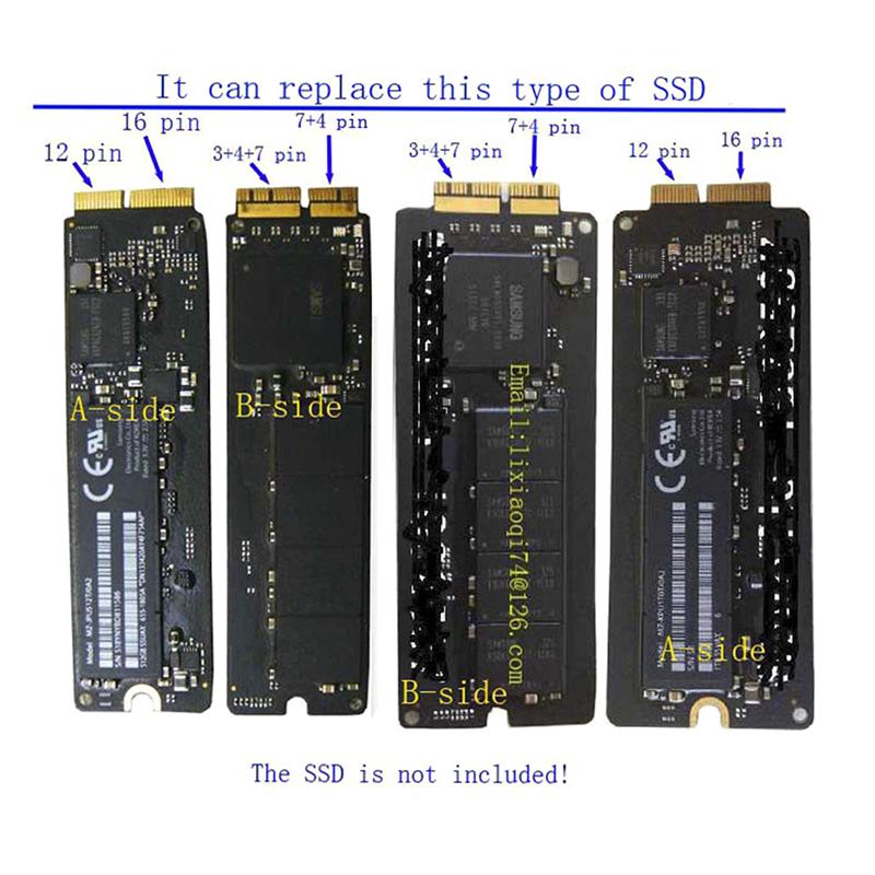
Verschiedene SSD-Steckverbindertypen auf Leiterplatten
It can replace this type of SSD 16 pin 7+4 pin 7+4 pin 12 pin 16 pin 12 pin 3+4+7 pin 3+4+7 pin A-side B-side Email: lixiaoq174@126.com B-side A-side The SSD is not included!
in „Mac Book Pro A1398. SSD weiterverwenden“ · PC Hard- und Software · · Platinenfotos
-
Datei
FMTuner.c
search_stop_level_high();//Setzt die erforderliche Signalstärke zum beenden // der Suche auf hoch // void High_Side_Injection(); //High Side Injection(???) // void Low_Side_Injection(); //Low Side Injection(???) // void PLLWert(long PLL); //Unterprogramm von SetFrequenz_kHz // long PLL_lesen (); //Unterprogramm von
in „[PIC] PIC 16F887 + I2C + Philips TEA5768HL RADIO“ · Mikrocontroller und Digitale Elektronik ·
-
PDF
tps5431.pdf
cycle. Finally, the PWM output is fed into the gate drive circuit to control the on-time of the high-side MOSFET. Overcurrent Limiting Overcurrent limiting is implemented by sensing the drain-to-source voltage across the high-side MOSFET. The drain to source voltage is then compared to a voltage level representing
in „Warum neigt ein (Stepdown) Regler mit Keramik Cs zum schwingen?“ · Analoge Elektronik und Schaltungstechnik ·
-
PDF
IDF_V30_Spec.pdf
system UNOWNED Outline can be modified in either system Record 2 Field, Description Type Value 1 Board side string TOP Outline applies to top side of board only BOTTOM Outline applies to bottom side of board only BOTH Outline applies to both sides of board 2 Outline height float Any (≥ 0) The outline height
in „Eagle 3D Darstellung“ · Platinen ·
-
PDF
Brauchbar_QC12864B.pdf
SCLK low pulse width tSLW Pin RS(SCLK) 300 — — nS SCLK rise/fall time tR F Pin RS(SCLK) — — 20 nS SID data set-up time tSDS Pin R/W(SID) 40 nS SID data hold time t Pin R/W(SID) 40 nS SDH CS set-up time tCSS Pin CS 60 nS CS hold time tCSH Pin CS 60 — — nS MPU write timing MPU read timing 深 圳 市 亚 斌 电
-
PDF
MOSFET_Treiber.pdf
measured under board mounted and still air conditions. Symbol Definition Min. Max. Units V B High Side Floating Supply Voltage -0.3 525 V S High Side Floating Offset Voltage VB- 25 VB+ 0.3 VHO High Side Floating Output Voltage VS- 0.3 VB+ 0.3 VCC Logic SupplyVoltage -0.3 25 V VIN Logic Input Voltage
in „MOSFET - Treiber“ · Analoge Elektronik und Schaltungstechnik ·
-
 Bild
Bild
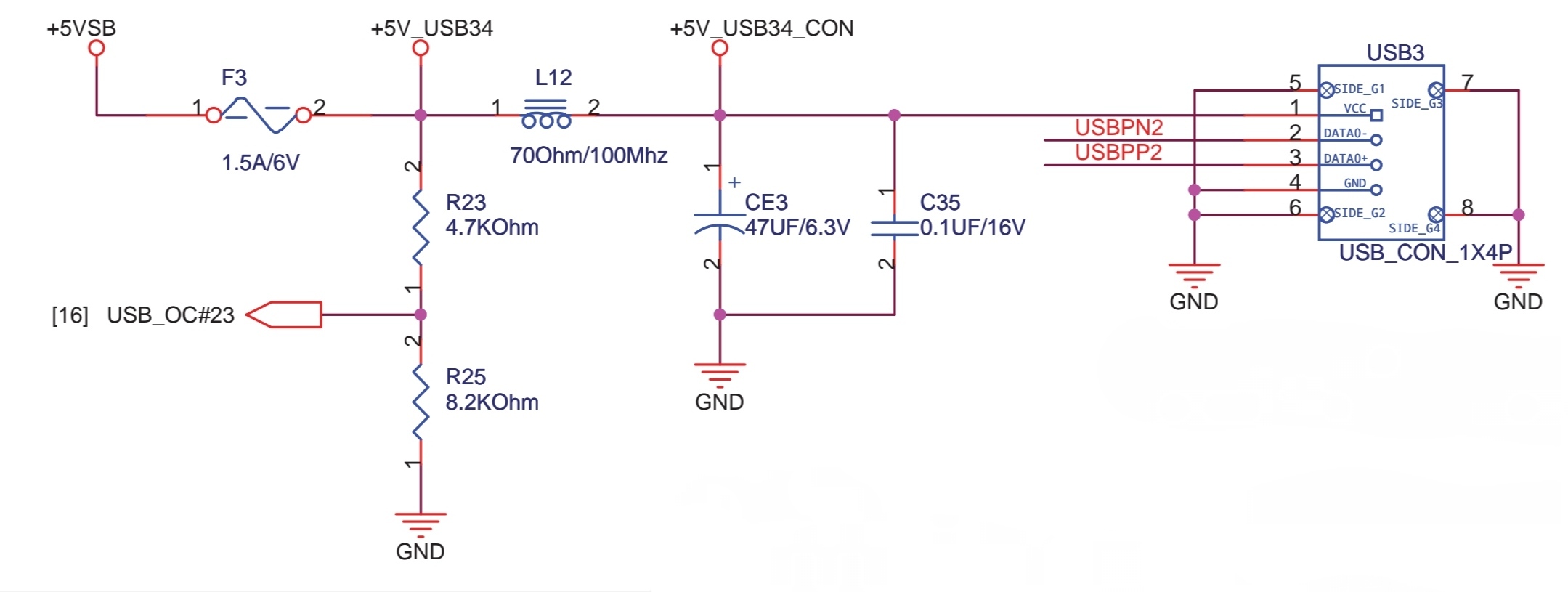
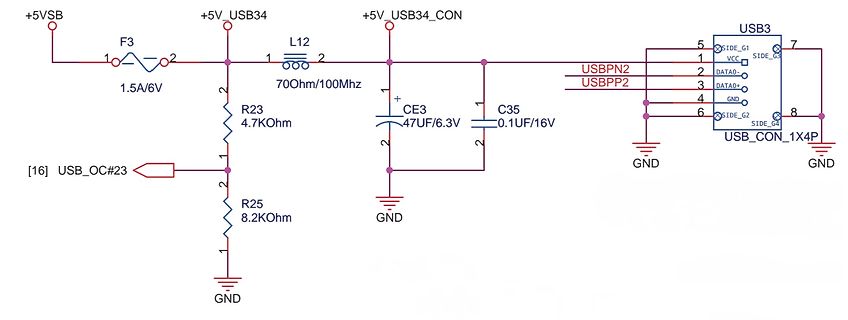
Schaltplan einer USB-Stromversorgung
5V_USB34_CON, R23, 4.7Kohm, CE3, 47UF/6.3V, C35, 0.1UF/16V, USB3, USBPN2, DATA-, DATA+, USBPP2, GND, SIDE_G1, SIDE_G3, SIDE_G2, SIDE_G4, USB_CON_1X4P, [16] USB_OC#23, R25, 8.2Kohm
in „USB-A Shield und Ground verbinden?“ · HF, Funk und Felder · · Schaltpläne
-
PDF
CM6206_Datasheet_v2.1_en.pdf
...........................................29 9.1 10K loading (Line Out / Surround / Center LFE / Side Surround) Frequency Response 29 9.2 10K loading (Line Out / Surround / Center LFE / Side Surround) Passband Ripple ... 30 9.3 10K loading (Line Out / Surround / Center LFE / Side Surround) THD+N Curve
in „soundchip mit mehr als stereo“ · Mikrocontroller und Digitale Elektronik ·
-
PDF
cm6206_2_3.pdf
.......................................... 28 9.1 10K loading (Line Out / Surround / Center LFE / Side Surround) Frequency Response 28 9.2 10K loading (Line Out / Surround / Center LFE / Side Surround) Passband Ripple....29 9.3 10K loading (Line Out / Surround / Center LFE / Side Surround) THD+N Curve
in „USB Stereo Eingang Mikro oder line-in“ · Mikrocontroller und Digitale Elektronik ·
-
PDF
cm6206_2_3.pdf
.......................................... 28 9.1 10K loading (Line Out / Surround / Center LFE / Side Surround) Frequency Response 28 9.2 10K loading (Line Out / Surround / Center LFE / Side Surround) Passband Ripple....29 9.3 10K loading (Line Out / Surround / Center LFE / Side Surround) THD+N Curve
in „PC Sound-Hardware: CD-Laufwerk“ · PC Hard- und Software ·
-
PDF
CM6206_Datasheet__v2.3_1_.pdf
.......................................... 28 9.1 10K loading (Line Out / Surround / Center LFE / Side Surround) Frequency Response 28 9.2 10K loading (Line Out / Surround / Center LFE / Side Surround) Passband Ripple....29 9.3 10K loading (Line Out / Surround / Center LFE / Side Surround) THD+N Curve
in „USB-Soundkarte zu einem Spannungslogger umbauen, wie die Eingänge schützen?“ · Mikrocontroller und Digitale Elektronik ·
-
PDF
HM303-5_Service_Manual.pdf
CRT-Board ............................................................... 16 CRT-Board (Top and Bottom side) ........................... 17 Power Supply (PS-Board)........................................ 18 PS-Board (Bottom side) .......................................... 19 PS-Board (Top side)...........
-
PDF
Si8931_32_analog_isolator.pdf
Si8931 Pinout (Top View) Table 1. Si8931 Pin Descriptions Name Pin Number Description VDDA 1 Input side power supply VIN 2 Voltage input NC1 3 NoConnect GNDA 4 Input side ground GNDB 5 Output side ground AON 6 Analog output low AOP 7 Analog output high VDDB 8 Output side power supply 1. No Connect.These
-
PDF
Tubes_Amplifier.pdf
has more than two output tubes, then the value measured must be divided by the number of tubes per side. In the case of an amplifier with four output tubes (two per side), the measured value must be divided by two. If six tubes are used, the value must be divided by 3, for 8 tubes, divide by 4, and so
in „Röhrenverstärker (Gitarre) - Röhrenstausch - Ruhestrom (BIAS) einstellen“ · Analoge Elektronik und Schaltungstechnik ·
-
PDF
an1827.pdf
Application Note 1827 Author: Ray Pilukaitis High-Side, High Current Sensing Techniques Introduction There is a need in many applications to sense currents on the high voltage op amp can be used in a standard differential high-side rail of a power bus and
in „Strommessung - Hohe Spannung, kleiner Strom!“ · Analoge Elektronik und Schaltungstechnik ·
-
PDF
EPCOS_AN_01_Principles_of_SAWR-stabilized_oscillators.pdf
The choke L1 can often be designed like a copper line on the PCB (without grounding to the wiring side). A transmitter antenna can thus be implemented. Oscillators with two-port resonators The typical oscillator circuit for two-port resonators is the Pierce oscillator. Fig.3: Pierce oscillator The amplifier
-
PDF
DOC40P_95P_125P_PARTS.pdf
PCB Connecting Wire (SWC) 1 6 23600006 Wire Retainer 3 7 2A35017C LLG Assembly 1 8 24300016C Right Side Plate 1 9 24300017C Left Side Plate 1 10 26500003C Roller Tension Spring 2 11 24400004C Roller 2 12 2A35010C Lower Heat Platen Ass’y 120V 1 12 2A35006C Lower Heat Platen Ass’y 230V 1 13 26300012C Pad
in „Laminator Unterlagen für HD320 PRO und GBC H200“ · Platinen ·
-
PDF
DRV8711.pdf
through the low-side FET and the opposite body diode. Which side of the bridge is tri-state and which one is driven low depends on the current direction on the previous step. The bridge with the high side that has been
in „DRV8711 Schrittmotortreiber Fehler“ · Analoge Elektronik und Schaltungstechnik ·
-
PDF
Datasheet_DRV8711.pdf
through the low-side FET and the opposite body diode. Which side of the bridge is tri-state and which one is driven low depends on the current direction on the previous step. The bridge with the high side that has been
in „DRV8711 Steppermotortreiber - Hohe Geschwindigkeiten“ · Analoge Elektronik und Schaltungstechnik ·
-
PDF
capacitance_sensing.pdf
Under Buttons ground plane plays an important role in setting Figure 6 shows details of the button side of the the capacitance of the button. This button circuit board. The non-button side of the board is capacitance is denoted as C in this Application not shown, but it is recommended that a metal fill
in „KICAD-Kupferfläche“ · Platinen ·
-
PDF
E461201_BA_Rev17_Touch-it_XELO.pdf
......................................................................11 2.3 Interfaces Connector Side (CPU T56N).....................................................................................................12 2.4 Interfaces Connector Side (CPU GX-415GA / i5-4300U).............................
-
 Bild
Bild
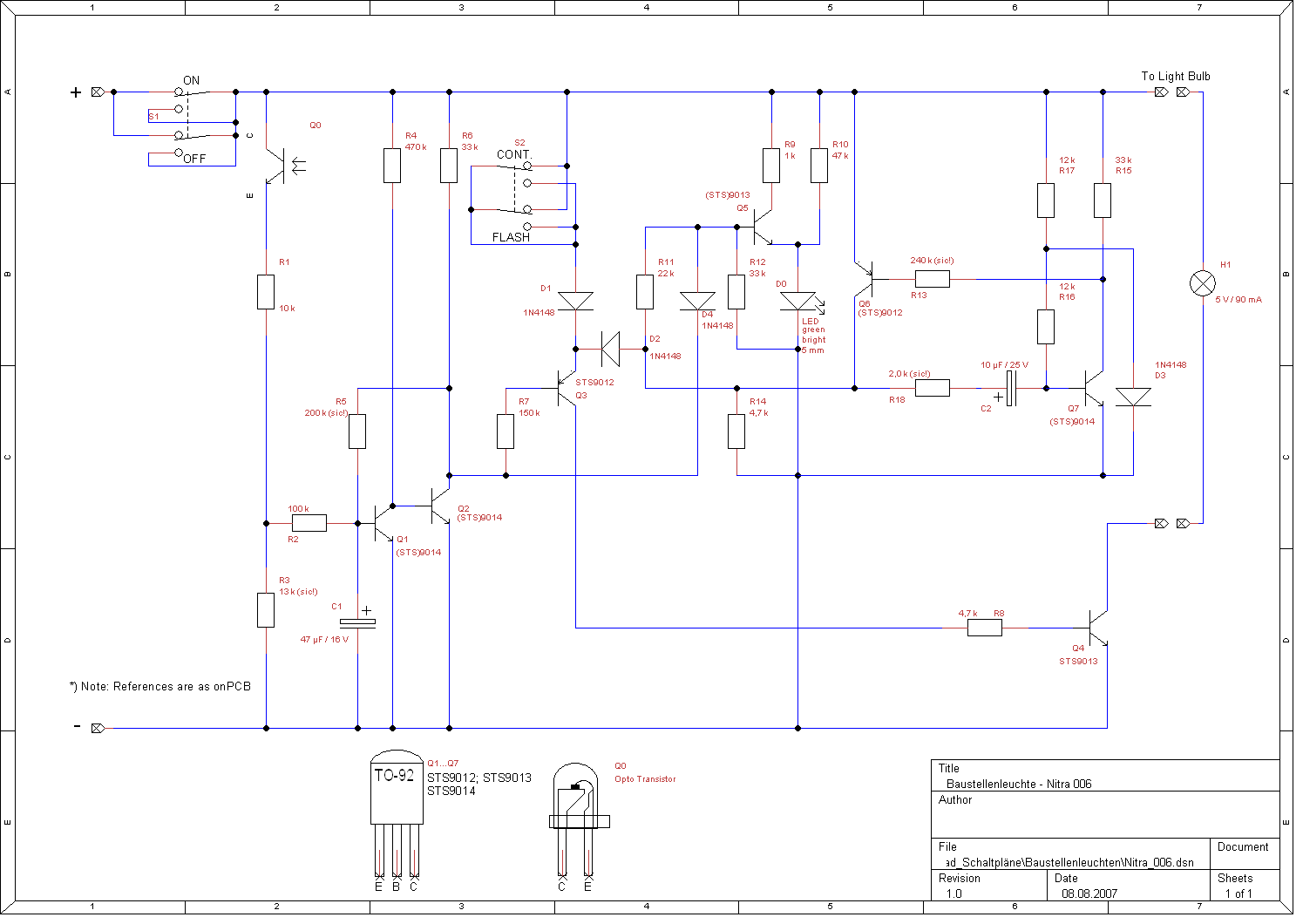
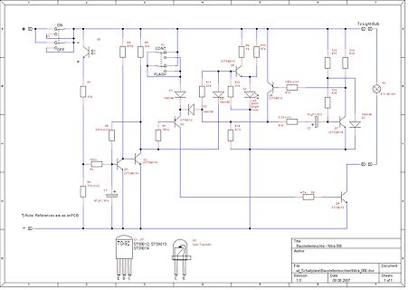
Schaltplan einer Bausteuchte
ON OFF Q0 R4 470k R6 33k CONT FLASH D1 1N4148 (STS)6013 Q5 R11 22k R12 33k R10 47k 240 k(sid) R17 12k R15 33k H1 5V / 90mA D2 1N4148 D3 1N4148 LED 5mm bright R13 12k R16 12k R18 2,0 k(sid) C2 10uF/25V Q6 (STS)6012 R7 180k Q3 (STS)6014 R14 4,7k R2 100k R3 13k (sid) C1 47uF/16V Q1 (STS)6014 Q2 R5 200k (sid) R8 4,7k Q4 STS9013 TC-92 STS9012 STS9013 STS9014 Q0 Opto Translator E B C C E Title Bausteuchten- Nitra 006 File kd_SchaltplaeneBausteuchtenNitra_006.dsn Revision 1.0 Date 08.08.2007 Sheets 1 of 1
in „Baustellenleuchte Blinkschaltung“ · Analoge Elektronik und Schaltungstechnik · · Schaltpläne
-
PDF
TD035STEB1_Product_Specification_Ver_03.pdf
LED Power Supply (+) 45 Cathode L - LED Power Supply (-) 46 GND - Ground 47 XR - Touch Panel Right Side Pin 48 YL - Touch Panel Lower Side Pin 49 XL - Touch Panel Left Side Pin 50 YU - Touch Panel Upper Side Pin 3.2 Touch panel Pin Touch Panel Module Symbol Description Remark Pin Pin 1 47 XR Touch Panel Right Side 2 48 YL Touch Panel Lower Side 3 49 XL Touch Panel Left Side 4 50 YU Touch Panel Upper Side Y U X L XR Y L 4 1 Pin Assignment for Touch Panel The information contained herein is the exclusive property
in „TFT ansteuern“ · Mikrocontroller und Digitale Elektronik ·
-
PDF
TD035STEB1_Product_Specification_Ver_03.pdf
LED Power Supply (+) 45 Cathode L - LED Power Supply (-) 46 GND - Ground 47 XR - Touch Panel Right Side Pin 48 YL - Touch Panel Lower Side Pin 49 XL - Touch Panel Left Side Pin 50 YU - Touch Panel Upper Side Pin 3.2 Touch panel Pin Touch Panel Module Symbol Description Remark Pin Pin 1 47 XR Touch Panel Right Side 2 48 YL Touch Panel Lower Side 3 49 XL Touch Panel Left Side 4 50 YU Touch Panel Upper Side Y U X L XR Y L 4 1 Pin Assignment for Touch Panel The information contained herein is the exclusive property
-
PDF
rt8279.pdf
82 15 22 x 2 8 100 18 82 22 22 x 2 Functional Pin Description Pin No. Pin Name Pin Function High Side Gate Drive Boost Input. BOOT supplies the drive for the high side 1 BOOT N-MOSFET switch. Connect a 10nF or greater capacitor from SW to BOOT to power the high side switch. 2, 3 NC No Internal Connection
in „Suche Schaltregler“ · Analoge Elektronik und Schaltungstechnik ·
-
PDF
STK681-332-E.pdf
or falling. H H L Forward (CW) No input signal is needed that turns off the H L H upper- and lower-side drive devices when Reverse (CCW) L H H switching the rotational direction. Brake L L L or H GND side MOSFET ON H H H V side MOSFET ON CC * Output control is enabled by applying an external PWM signal
in „Thermische Berechnung bei H-Brückentreiber“ · Mikrocontroller und Digitale Elektronik ·
-
PDF
CLAA070VA02.pdf
............................... P11 7. MECHANICAL SPECIFICATION ………………...………………………… P12 (a) Front side .................................................................................... P12 (b) Rear side ..................................................................................... P12 8. OPTICAL
in „Wer kennt diesen Display-Fehler? (Typisch?)“ · Mikrocontroller und Digitale Elektronik ·
-
PDF
DometicColdMachine50-54-55-84-85-86-94-95-96-CS-NC15_IOM_4445100001_EMEA16_20xx-xx-xx.book.pdf
VD-16 i samsvar medfig. 9,side 6. ➤ Tilkoble andre fordamperei samsvar medfig. i,side 9. Nøklertilillustrasjonene Nr. ifig.8,side5 Forklaring 1 Likestrømsvifte 2 Termostatknapp NO 235 Nr. ifig.9,side6 Forklaring 1 Tilkoblingskabel Nr. ifig.0,side6 Forklaring 1 Tilkoblingskabel Nr.i fig.i,side9og Forklaring fig.j,side 9 1 Koblingsblokk 2 Kompressor 3 Vifte 4 Bryterfig. i ellerTEC-kontrollenhetfig. j PASSPÅ! Isolerog tettveggåpningene forsiktig
in „Schaltsymbol“ · Fahrzeugelektronik ·
-
PDF
lt1157.pdf
LTC1157 3.3V Dual Micropower High-Side/Low-Side MOSFET Driver U F EA U T RE S DESCRIPTIO Allows Lowest Drop 3.3V Supply Switching TheLTC1157dual 3.3VmicropowerMOSFETgatedriver Operates on 3.3V or 5V Nominal Supplies makes it possible to
in „3V Gate-Treiber gesucht“ · Analoge Elektronik und Schaltungstechnik ·