AT89C51RC NONE No Need WPGM51 V5.70 ATMEL MPU/MCU AT89C51RC2 NONE No Need WPGM51 V5.70 ATMEL MPU/MCU AT89C51RD2 NONE No Need WPGM51 V5.70 ATMEL MPU/MCU AT89C51SND1 ADP-T89C51SND1-BG/PL/Q No Need WASIG V5.65
äußerst bedienerfreundlich nur für Gewerbetreibende 1-48 Lagen Leiterplatten und SMD-Schablonen, ab 1AT Express, seit 30 Jahren Standard 2L: 4AT Produktionszeit, 4L: 5AT Produktionszeit, 6L & 8L: 6AT Produktionszeit Standard: 0.1mm Leiter, 0.2mm Bohren Preiswerte Spar-Option ab 8AT Inklusive: Kompletter
GmbH (10AT, immer mit LS.+E-T.) 46,41 73,07 HAKA Elektronik-Leiterplatten GmbH 64,54 106,13 LEITON 54,98 104,51 MME-Leiterplatten (200µm Leiter) 41,44 ? PCB Pool 50,27 100,54 Q-print/Q-PCB 55,62 95,89 mit Lötstopp
simple serial method Input SDSEL Upper screen HOD, ED ED HOD, ED ED Lower screen ― ― LOD, ED ED ce0 ce0 at DUAL = H Chip enable pin for display memory in the address range 0000H to 07FFH Output (LOD) LOD at DUAL = L Serial data output for odd columns in lower area of LCD ce1 at DUAL = H Chip enable pin for
main switch. . . . . . . . . . . . . . . . . . . . . . 50 2.7.1 Placement system switched off at the main power switch, but still connected . . . . . 51 2.7.2 Placement system switched off at the main power switch and disconnected . . . . . . 51 2.7.3 Compressed air conditions in the machine after
gains are modest. For a 5 V, 2 A design the external diode adds t t 1 2 ~0.1% to full load efficiency at 85 VAC and ~0.2% at 230 VAC. PI-8394-051818 The voltage rating of the Schottky diode and the SR FET should be at Figure 15. Unacceptable FORWARD Pin Waveform before Handshake with Body least 1.4 times
46 C707 T 168 16 C844 T 44 69 C1005 B 98 35 L901 T 108 106 R215 B 96 73 R701 T 178 22 D1100 T 176 51 C320 B 128 44 C708 T 171 24 C845 T 43 69 C1006 B 96 39 D1200 T 88 97 L902 T 72 55 R216 B 87 62 R702 T 176 15 C321 B 122 48 C709 T 172 11 C846 T 47 69 C1007 B 89 34 D1201 T 184 73 L903 T 66 99 R217 B
is optimized for use in many AT24C01A industrial and commercial applications where low power and low voltage operation are essential. The AT24C01A/02/04/08/16 is available in space saving 8-pin PDIP, AT24C02 (AT24C01A/02 /0 4/08 /1 6), 8-Pin MSOP (AT24C01A/02), 8-Pin TSSOP (AT24C01A/02/04/08/16), and 8-Pin and 14-Pin JEDEC SOIC (AT24C01A/02/04/08/16) packages and is accessed via a 2-wire serial interface. In AT24C04 addition, the entire family is
frequency (1/f) noise is also improved by the chopping technique. Instead of increasing continuously at a 3dB/octave rate, the internal chopping causes noise to decrease at low frequencies. Cexte |1 U NTEXT Cexta [2] [13] CLK IN NCIGUARD) | 3 | 112] CLK OUT 4in [ 5} 10] OUTPUT NCIGUARD) [ 6| 3] output
logic ‘1’. Consequently, a logic ‘1’ appears at the output of the gate for this short period until the other input isat logic ‘1’ ;i.e.the condition for ’0’ output. : At the end of the comparator pulse, the input with the shorter delay returns to
at a certain angle with respect to the light input window, so the sensitivity is affected by the polarization com- ponents if the light enters without any countermeasure. Figure 4-51 indicates that the
7 AN1543/D VCC ΣR Lp tube I + SR (14) At the same time, the voltage across the capacitor is maximum as stated by Equation 15: VC= V CC*Q (15) HALF FLUORESCENT The behavior of an R/L/C resonant circuit is depicted by VPP
Hi! Benötigt wird DIL40. Ich hätte sonst auch AT89S... als DIL da. Roger P. schrieb im Beitrag #7981985: > Will die wegwerfen.... Ach so. :o) Versuch es doch hier im Markt! Gruß Jobst
Videotextdecoder ist. Das wird aber spätestens beim verifizieren auffliegen. Ich teste hier mit AT89S52. Gruß Jobst
and series inductors LP in alternating order. The other filter classes can be derived from it: In a high-pass filter: 1 C LP → L HP = 2 (16.35) ωB·C LP 1 L LP → C HP = 2 (16.36) ωB·L LP 222 In a band-pass filter: C → parallel resonance circuit with (16.37) LP CLP CBP = (16.38) ∆Ω ∆Ω LBP = ω1·ω 2C LP (16.39) LLP → series resonance circuit with (16.40) ∆Ω CBP = (16.41) ω1·ω 2L LP L LBP = LP (16.42) ∆Ω In a band-stop filter: CLP → series resonance circuit with
output power, programmable up to + 22 dBm (RFO_HP) • low output power, programmable up to +15 dBm (RFO_LP) In an application, the customer can choose to use an RF output (RFO) or both RFOs, using a DC switch for biasing circuit. Note: Only one RFO can be used at a time. When using one RFO, only one RF Tx
R5F56108VNFP B SOFTWARE: SYSTEM EXPLODED f C36f CY920 MODULE ASSY B Be sure to replace the NFC module at the same time. Procedure after Replacement A : The software has been written. The software is not written at the time of replacement. B : The software has been written. The software may need to be rewritten
Eckhard T. schrieb im Beitrag #7935422: > Handelt es sich um einen AT89C52 oder eine der AT89C52R.. Versionen? > Letztere lassen sich ggf. leicht seriell programmieren und auslesen. Du meinst wohl eher den AT89S52. Einen AT89C52R* gibt es nicht. Und der AT89C51RC
ist nicht seriell > programmierbar. Danke für die Korrektur. Ich war bei den AT89C51Rx2-Typen, die sich mit dem erwähnten Flip über eine serielle Schnittstelle programmieren lassen. Ich hatte vor einiger Zeit mal viel Spaß mit den „kompatiblen“ LP51-Typen.
0018 ??_AT89C51RD2_ NUMBER 001B ??_AT89C51_ NUMBER 0015 ??_AT89C52_ NUMBER 0016 ??_AT89C55WD_ NUMBER 0017 ??_AT89LP2052_ NUMBER 0001 ??_AT89LP213_ NUMBER 0003 ??_AT89LP214_ NUMBER 0004 ??_AT89LP216_ NUMBER 0005 ??_AT89LP4052_ NUMBER 0002 ??_AT89LP428_ NUMBER 0006 ??_AT89LP52_ NUMBER 0007 ??_AT89LP6440_ NUMBER 0009 ??_AT89LP828_ NUMBER 0008 ??_AT89LS51_ NUMBER 0011 ??_AT89LS52_ NUMBER 0012 ??_AT89S2051_ NUMBER 000A
Thomas Z. schrieb im Beitrag #7897918: > Das ist ganz sicher kein 80c49 Assembler Quelltext sondern 80c51. Dann könnte man ja den AT89LP51RD2-20PU nehmen. Der hat einen UART-Bootloader, d.h. man braucht kein extra Programmiergerät dafür. Nur einen USB To RS232 TTL Converter Adapter. https://www.amazon.de
output power, programmable up to + 22 dBm (RFO_HP) • low output power, programmable up to +15 dBm (RFO_LP) In an application, the customer can choose to use an RF output (RFO) or both RFOs, using a DC switch for biasing circuit. Note: Only one RFO can be used at a time. When using one RFO, only one RF Tx
read from, or written to, the port that generated the interrupt. Resetting occurs in the read mode at the acknowledge bit after the rising edge of the SCL signal, or in the write mode at the acknowledge bit after the high-to-low transition of the SCL signal. Interrupts that occur during the acknowledge
0 0 standard C51 port 1 - 0 LED0[1,0] 0 1 2 mA current source when P3.6 is at Low Level 1 0 4 mA current source when P3.6 is at Low Level 1 1 10 mA current source when P3.6 is at Low Level Reset Value = XXXX 0000b 57
Michael schrieb im Beitrag #7830683: > Peter D. (peda) schlägt den AT89C2051 vor. Vorschlagen würde ich ihn nicht mehr. Ich wollte nur darlegen, daß man schon mit sehr wenigen Ressourcen Zeiten und Frequenzen genau messen konnte. Es gibt als Upgrade den AT89LP4052 oder AT89LP51RD2 und der Wickenhäuser und SDCC sollen wohl auch recht guten Code erzeugen.
0 0 standard C51 port 1 - 0 LED0[1,0] 0 1 2 mA current source when P3.6 is at Low Level 1 0 4 mA current source when P3.6 is at Low Level 1 1 10 mA current source when P3.6 is at Low Level Reset Value = XXXX 0000b 57
at the end of the output cable when the power supply is A large anode area can increase high frequency radiated EMI. delivering maximum power. The output voltage at the terminals of the supply is the value
approximately 135mW at the input. The LP2951 chip (U15 in Figure 58) also generates an error signal VoltErr, if the input voltage *VZK* is too low to regulate the set output voltage. This error signal is low active and transferred
CPU is executing MRET, the value of mpte is automatically popped back into this. Espressif Systems 51 ESP32-C3 TRM (Version 1.1) Submit Documentation Feedback 1 ESP-RISC-V CPU GoBack Register 1.26. mcontrol (0x7A1) d) d) d) d) d) rv de re rv n rv h rv ut (rs mo (se i (rs ci (rs at (rs xe toeoa d h a
nur noch unter DOSBox laufen. Man braucht auch kein großes Entwicklungsboard mehr, ein AT89C51RB2 hat alles onboard. Mit Flip lädt man ein Programm über die UART in dessen Flash. https://www.digikey.de/de/products/detail/microchip-technology/AT89C51RB2-3CSUM/1245778 Die MCS51 lassen sich
NMOS waren. Noch zu DDR-Zeiten gab es CMOS-SRAM (U6516) im Bastlerladen. Damit habe ich dann später AT89C51 erweitert. Der 6516 hatte das nötige Adreßlatch ja schon eingebaut.
CPU is executing MRET, the value of mpte is automatically popped back into this. Espressif Systems 51 ESP32-C3 TRM (Version 1.1) Submit Documentation Feedback 1 ESP-RISC-V CPU GoBack Register 1.26. mcontrol (0x7A1) d) d) d) d) d) rv de re rv n rv h rv ut (rs mo (se i (rs ci (rs at (rs xe toeoa d h a
??_AT89LP3240_ NUMBER 000A ??_AT89LP4052_ NUMBER 0002 ??_AT89LP428_ NUMBER 0006 ??_AT89LP51ED2_ NUMBER 0011 ??_AT89LP51IC2_ NUMBER 000E ??_AT89LP51ID2_ NUMBER 0010 ??_AT89LP51RB2_ NUMBER 000C ??_AT89LP51RC2_ NUMBER 000D ??_AT89LP51RD2_ NUMBER 000F ??_AT89LP51_ NUMBER 0007 ??_AT89LP52_ NUMBER 0008 ??_AT89LP6440_ NUMBER 000B ??_AT89LP828_ NUMBER 0009 ??_AT89LS51_ NUMBER 0019 ??_AT89LS52_ NUMBER 001A ??_AT89S2051_ NUMBER 0012
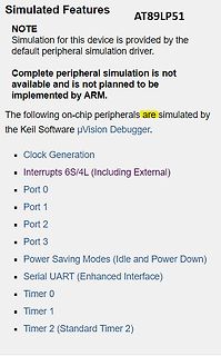
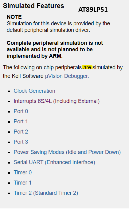
Simulated Features
AT89LP51
NOTE
Simulation for this device is provided by the default peripheral simulation driver.
Complete peripheral simulation is not available and is not planned to be implemented by ARM.
The following
uVision Debugger (5.38.00 Eval Version) kommt in der Simulation nicht mit PowerDown klar, wenn ich den AT89LP51RB2 als Device verwende. Diese simple Loop kann ich im Single Step (F11) durchgehen, obwohl beim PCON |= 2 die Simulation sofort anhalten sollte, weil die Clock steht. [code] int count = 0; void
Aussagen von Keil zu den beiden Chips. Daraufhin hatte ich angenommen, PD geht in der Simulation beim AT89LP51.
https://www.silabs.com/developers/keil-pk51 Du kannst bei Silabs / Keil auch eine vollwertige Keil Lizenz bekommen.
sowieso nicht möglich ist, werde ich auch nicht versuchen, da durchzusteigen. Habe mir jetzt den Atmel AT89LP51RB2 ausgesucht, ist bei Mouser verfügbar. Der wird ordentlich von Keil supportet und kann weit mehr, als ich benötige. Zumindest konnte ich schon erste Simulationen erfolgreich durchlaufen.
protected EEPROM block beginning at selected address Read data from the protected EEPROM block beginning at the selected IDREAD 0011 0011 address CLRRAM 0101 0100 Clear all SRAM data to ‘0’ DS20002300E-page 10 2012-2023 Microchip Technology
LOOPBACK Near-end (Remote) loopback is conducted at PHY port 1 of the KSZ8851SNL. The loopback path starts at the PHY port’s receive inputs (RXP/RXM), wraps around at the same PHY port’s PMD/PMA, and ends at the PHY port’s transmit outputs (TXP/TXM).
leider Philips/NXP seine 8051 mit I2C vollständig abgekündigt. Eine Umrüstung auf Atmel ATmega8 und AT89LP51RD2 ist dann gründlich in die Hose gegangen, die sind definitiv nicht als Multimaster geeignet. Mit Haufen Timeouts, Retries ging eine Notlösung, allerdings mit unterirdischen Antwortzeiten. Wir
befüllt. Wir haben aber noch zusätzlich einen Message-FIFO im SRAM angelegt. Später haben wir den AT89C51CC03 und den AT90CAN128 verwendet. Der CAN-Controller ist bei allen 3 gleich aufgebaut, d.h. auch 15 MOBs. Zur Programmierung gibt es nicht viel zu sagen. Man setzt die Timingregister für die
selbst, vier LED-Displays mit gemeinsa- mer Kathode (TLR 324 von Toshiba) und einem Mikrocontroller AT89C2051 von Atmel(eswärenauchandereTypendenk- bar) istnur noch ein Temperatursensor er- forderlich. Der dafür gewählte LM75 von National Semiconductor passt sehr gut zum Rest der Elektronik, da er ebenfalls

 Bild
Bild