---------------------- --------------- V IN(min)– Vsat V IN(min)– Vsat – VOUT V IN – Vsat (t + t ) max 1/f 1/f 1/f on off min min min C 4.5x10 t5 4.5x10 t5 4.5x10 t5 T on on on I 2I [(t /t )+1] 2I 2I [(t /t )+1] PK(switch) out(max) on off out(max) out(max) on off R 0.3/I 0.3/I 0.3/I SC PK(switch) PK(
character generator ROM (code 0101) T6963C−0101 is built in as standard. ▯External display memory : 64 KB Max The addresses in display memory of the text area, graphic area and external character generator area are determined by software. ▯Read or Write operations from the CPU do not disturb the display. ▯A
/i key + print information: p/p key + Target weight z/T key Set Setp Min weight value S – min Max weight value S + max Tolerance ranges when values entered via keypad: or Delta min d – d min Delta max d + d max Numeric entry: Numeric keys 0–9 Enter parameters and . + z/T key for “Weight” Target
Geeignete bzw. passende Typen wären beispielsweise: MCP6022 (Rail-to-Rail, 2,8 MHz, 7 V/µs, allerdings max. 6 V Versorgung → nicht geeignet für ±15 V) OPA197 – passt sehr gut: Versorgung: ±2,25 V bis ±18 V Rail-to-Rail-Ausgang GBW: 10 MHz Slew Rate: 20 V/µs OPA192 Versorgung bis ±18 V Rail-to-Rail Ein- und
6.13.4 Replacing the limit switches for the end position of the width adjustment system (00365108-02) 197 6.13.5 Adjustment unit for the width adjustment system . . . . . . . . . . . . . . . . . . . . . . . . . 200 6.14 Light barriers and stopper for scanning the PCB positions along the transport routes
over recommended operating conditions (unless otherwise noted) PARAMETER TEST CONDITIONS MIN TYP † MAX UNIT VIT+ Positive-going input threshold voltage 750 900 mV See Table 1 VIT– Negative-going input threshold voltage 500 650 mV Vhys Hysteresis voltage IT+ – IT–) 100 VOH High-level output voltage –6
vor der eigenen Türe! An den TO hier mit WIN7, versuch es mal mit Google Chrom, da geht wohl die max 109er Version, der FF ist eh zu systemlastig und hat auch so seine Eigenheiten. Oder einen alten Browser wie MyPal-68, nicht den 74er, mit etwas Probieren kommt man damit auch weiter. Aber Onlinebanking
Mozilla\Firefox\Profiles\48d pdqqb.default-1523012017786\storage\archives\0\2025-11-13\default\https+++197a72 65ced95622a197ff33ef503784.safeframe.googlesyndication.com^partitionKey=%28https %2Ckreuzwortraetsel.de%29\idb\12183338011.files ist zu lang. Der Verzeichnisname C:\Users\berres\AppData\Roaming
Than MAX_FL Bytes and Bad CRC Statistic Register (ENET_RMON_R_JAB)....... 2053 57.5.71 Reserved Statistic Register (ENET_RMON_R_RESVD_0).......................................................................
Sicherheit Unmengen an verschiedenen Ausführungen, von denen die allermeisten mit der Urversion von Anno 197x nicht mehr allzu viel gemein haben. Außer der Pinbelegung bei TO-220. Und dementsprechend wird es auch sehr unterschiedliches Regelverhalten und Schwingneigung geben.
> Leider überhitzt der Spannungsregler L7805 Wohl etwas auf Kante genäht bei Uin 24V: Umin U max am Eingang μA7805C 7V - 25V. Und der Kühlkörper ist eher zur Zierde da mit seinen 21 Grad pro Watt. Aber das stand oben ja schon. Wie ist der überhaupt befestigt? Angenietet? ciao gustav
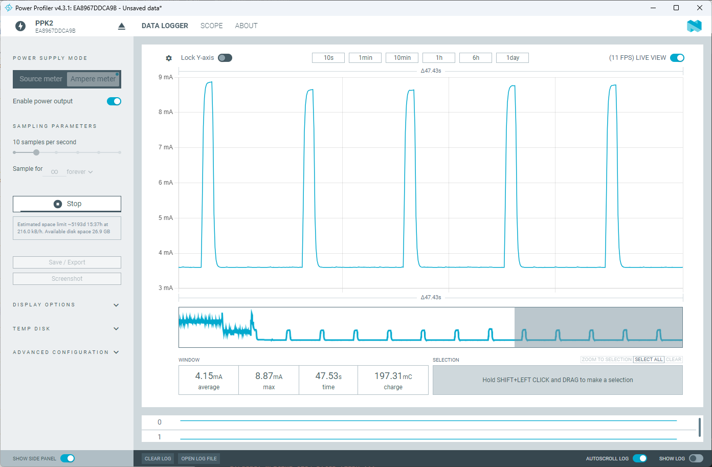
DISK ADVANCED CONFIGURATION WINDOW SELECTION ZOOM TO SELECTION SELECT ALL CLEAR 4.15mA average 8.87mA max 47.53s time 197.31mC charge Hold SHIFT+LEFT CLICK and DRAG to make a selection SHOW SIDE PANEL CLEAR LOG OPEN LOG FILE AUTOSCROLL LOG SHOW LOG
routine examines the Rdown and Rup bits in the range control status register. Ifthe range > range max. then the instrument must range up. Ifthe range < range min. then the instrument must range down. Italso ensures that in the TRIGGER LEVEL function only manual ranging isallowed. 1.4.1.4. M e a s u
measure anode luminous sensitivity) VOLTAGE 0 V ON LIGHT LEVEL OFF 5 6 7 8 9 (minutes) 1 µA ANODE I max. OUTPUT Ii I min. OR Ii I max. I min. 5 6 7 8 9 (minutes) WARM-UP PERIOD (5 minutes or more) THBV4_0440EA Figure 4-40: Light hysteresis In light hysteresis test, the photomultiplier tube is operated
auf. Habe nach Service manuals geguggt. Eines mit 158 Seiten habe ich. Das Benutzerhandbuch mit 197 Seiten habe ich auch. Das mit Bios-Batt und Start länger als ne Minute ist auch versucht wworden. Prozessor glaub ich nicht, weil ja schon mal an war. Hat jemand ne Idee?
räumlich da reinpassen. Nur makl Test. Am 330uF im eingelöteten Zustand, Karte vor mir, habe ich max. 1,8Ohm. Könnte aber auch der Nvidia Chip sein. Wobei da noch ein Switch ist. Edit: Es sind insgesamt 3 stk. 330uF. 2 stk. vor dem Switch, einer danach irgendwo. Die beiden vorderen haben (eingebaut
packaging E1 D 2 n 1 α E A A2 L c A1 β B1 p eB B Units INCHES* MILLIMETERS Dimension Limits MIN NOM MAX MIN NOM MAX Number of Pins n 8 8 Pitch p .100 2.54 Top to Seating Plane A .140 .155 .170 3.56 3.94 4.32 Molded Package Thickness A2 .115 .130 .145 2.92 3.30 3.68 Base to Seating Plane A1 .015 0.38 Shoulder
needed in order to keep the junction temperature below the manufacturer’s recommended value, T (J)max Calculate the total theta, θ(°C/W), needed. (T - T ) q JC= (J)max A(max) PD (150 40 ) q JC= 1.4 q JC= 78 ° / W (8) Now choose a device package with a theta at least 10% below this value to account for
, y a PARTNUMBER/STANDARDCONFIGURATIONS W a Numberof “A” “B” “C” y (10,16) “A” PartNumber Contacts Max. Max. Max. R Max. Max. 1.100 .900 .700 3 514-AG21D 14 (27,49) (22,86) (17,78) 2 . 1.220 1.010 .800 n “C” (2,54) “B” 516-AG21D 16 (30,99) (25,65) (20,32) , Max. Typ. Max. g r e i Note: Before ordering
devices. Dynamicrangeofdevicesforgeneral-purposeuse Application circuits Application circuits for theTOTX197 andTORX196, a pair of transmission and receiving modules for general-purpose use, are shown in the figure on the insertionsideonnector insertionsideonnector right.For theTOTX197 transmission module,
relative description 0.85 Oct, 2023 3. delete the description about 1/2 Bias and pull-down 4. Modify Max. value of TotalAccuracy and Integral Non-Linearity of ADC Electrical Characteristics 5.Add SOP-14 and change PA2 as PB0 in MSOP-10 and DFN-10 1. Update Electrical Characteristic 0.86 Oct, 2023 2. Modified
EV083(1).docx of JHLin 0.84 Aug, 2023 0.85 Aug, 2023 1. Modify the timing diagram of ADC 1. Modify Max. value of Total Accuracy and Integral Non-Linearity of ADC Electrical Characteristics 2. Add the table of “EEPROM Characteristics” 3. Add subsection for the section of “PWM Trigger ADC” 4. Add description
and V ds being the intrinsic drain-source voltage. The charge and capacitances are: for V > V new max 168 V max Vnew − V max Q gs = Cgs0· 2·Vbi 1 − 1 − + (11.364) V bi 1 − VVax bi ∂Q gs C gs0 ∂Vnew = · (11.365) ∂Vgs 1 − VVax ∂V gs bi ∂Q gs C gs0 ∂Vnew = · (11.366) ∂Vgd 1 − VVax ∂V gd bi and
▯ } I ( ▯ 2 › 2 LED Driver IC ▯ D O ▯ î C ▯ +12V_FAN LED Forward Voltage E 2 2 1 1 SDICS ▯ +15V R_Max 2.4V x 4 pcs = 9.6V L L L L SDI_CLKL ) For EMI ▯ 3 3 3 2 2 2 1 1 1 G_Max 3.3V x 4 pcs = 13.2V C227 C100p50N0402 LED1_G L L L L L L L L L Pin Definerd 6 5 4 3 2 1 O ▯ C567 C100p50N04N2 LED1_R B_Max 3.3V
power dissipated by the device will be equal to: batteries which can be plugged in backward. I OUT(MAX)(VIN(MAX) – VOUT) + GND (VIN(MAX)) The output of the LT1763-X can be pulled below ground where, withoutdamagingthedevice.Iftheinputisleftopen-circuit I = 250mA or grounded, the output can be pulled below ground by OUT(MAX) 20V. For fixed voltage versions, the output will act like a V IN(MAX) = 6V largeresistor,typically500korhigher,limitingcurrentflow I GND at (OUT = 250mA, V IN6V) = 5mA So, to less than 100µA. For adjustable
target -m be changed by the end user) device; for example, 6 Worst case conditions used (from Slow/max data Fast/min data data in speed grade file) Fast/min clock Slow/max clock Timing Closure 21 Timing-Driven Flow Using Lattice Diamond Design Software Table 2: Performance Grades and PAR Behavior
3ECEMBER 197 ALPHANUMERIC Displays 64 Character ASCII Set and Special Characters 16 SEGMENT FONT PLUS CENTERED D.P. 3.81mm (0.150")CHAHACTEH HEIGHT APPLICATION FLEXIBILITY WITH PACKAGE DESIGN 4 and 8 Character Dual-In-Line
permanent damage if exceeded. Parameter Symbol Value Units DC supply voltage range (pin 8, = 20mA max) V -0.3 to 25.0 V CC CC Continuous DC supply current at V pin (V = 15V) I 20 mA CC CC CC ASU output (pin 4) -0.3 to 19.0 V OUTPUT (pin 6) -0.3 to 20.0 V V input (pin 1, I ≤ 10mA) -0.7 to 4.0 V SENSE
noch eine gewisse Anzahl analoger Oszilloskope an. Das Angebot beschränkt sich häufig auf Geräte mit max. 20 MHz Bandbreite, die für Schulen und Ausbildung angeboten werden. Das Aussterben analoger Oszilloskope geht soweit, dass mittlerweile DSOs angeboten werden die von der Funktion und dem Formfaktor
Peaktech 389 2 500 100 8 10M USB und LAN Anschluss, 40V SS bei USB, 400V SS bei LAN P 1290 Peaktech 197 2 100 25 8 5k 400V SS galv. Trennung zu USB DSO-2090 USB Hantek - Qingdao Hatek Electronic Co., Ltd. 200 2 50 100 40 8 32k 64k Wenige Vorteile gegenüber einem Tischgerät. Analogbandbreite bei der Samplingrate
Ausgangsspannung ( = Gatespannung) hoch auf pos. Maximalwert. Damit ist die Gate-Source-Kapazität max. aufgeladen. Wird die Last wieder eingeschaltet, führt der Fet erst einmal maximalen Strom, bis die Gate-Source kapazität auf stationären Wert entladen ist. Daher ein Stromspike. Es werden hier sicherlich
dt/stability/stability.html MIC920 (5-18V 3000V/us 80MHz Micrel) LTC6260 (1.8-5.25V, 20uA 400uV) OPA197/2197/4197 (36V 1nF 20V/us 100uV) MAX4162/MAX4163/MAX4164 (2.5-10V any) und MOSFET mit geringer Gate-Kapazitat bei trotzdem grosser SOA ist natürlich Grundvoraussetzung.
Hcimcmpriingcr der unteren Preisklasse mit einern enISI)TI.:chcnJI]e~ricbssp:lnnungsbl'rcjc\'on 4,.5 ... 15V (max. 16V) konzipierl. Abweichend von den üblichen Gehäuse varianten. befindet~icsich in einem 22poJigen DIL·Plastgchiiuse mil dem Rcihcnabsland l(lmm. Ocr für deli A .J/OO 0 geltende TYPSlölndard ist in
: 74h Size: 8 bits Table 3-213 Lock Count Bit Access Symbol Description [7:4] R/W locked_cnt_noisy_max These bits set the max value of the hlock sensor for noisy signals. 8 is added to this value. Default = 7 stands for 15. These bits set the max value of the hlock sensor for clean signals. 8 is [3:0] R/W locked_cnt_clean_max added to this value. Default = 4 stands for 12. 3.9.18 H Loop Max State Address Offset: 17h Access: Read/Write Default Value: CBh Size: 8 bits 83 电子专业技术主页: HTTP://WWW.LCDHOME.NET 资料收藏: 版权归原作者所有 谨供学习用
Typical Weight: 6.8 grams (0.22 oz.) mm (inches) Typical Volume: 2.4 cubic centimeters (0.14 cubic inch) Max Rev Charge: 1 microampere Energy Density: 183 milliwatt hr/g, 647 milliwatt hr/cc Typical Li Content: < 0.3g Operating Temp: -30C to 60C Self Discharge: ~1% / year 24.50 (0.965) 3.45 (0.136) Ref. 24.30 (0.957) 3.15 (0.124) Ref. Safety: R1.25 (0.049) Ref. 22.0 (.866) 1.00 (0.039) Ref. Max Minimum (1) KEEP OUT OF REACH OF CHILDREN. Swallowing may lead to R0.75 (0.030) Ref. serious injury or death in as little as 2 hours due to chemical burns and 5.00 (0.197) potential perforation of the
A .50 mA Hipot rating (one minute): Line to Ground: 2250 VDC Line to Line: 1450 VDC Rated Voltage(max.): 250VAC S Model Operating Voltages: LINE LOAD Selectable or Fixed 115/230 VAC Operating Frequency: 50/60 Hz Rated Current: Non-Filtered – 10A Filtered – 3, 6 or 10A L Model Fuseholder: Accepts one
20 A1, Frequenz- Smart PLGS 2012 A1. leistung.......≤20dBm Frequenzband ..2400-2483,5MHz Temperatur.max 50 °C Ladevorgang 0 - 10 °C, bzw. 50 - 60 °C bei einem Ladestrom von max. 4 A 10 - 50 °C bei einem Ladestrom von max. 12 A Betrieb......-20 - 50 °C Lagerung 8 DE AT CH Ladezeit Akku Smart PAPS 208 A1
µA Fluke 289 (50,000 count) $950 1.8mV / mA 0.1mV / µA Gossen MetraHit E-XTRA (60,000 $1700 300mV max 150mV max count) Fluke 8808A (5.5 digit) $1100 1mV / mA 1mV max Fluke 8846A (6.5 digit) $2100 500mV max 15mV max Keithley 197A Microvolt (5.5 digit) N/A 300mV max 300mV max As you can see from the table
Brocks [1992: Plastizität - Grundlagen und Anwendungen für Ingenieure. Vieweg, Braunschweig. J. Betten [197: Ein Beitrag zur Invariantentheorie in der Plastomechanik inkompressibler isotroper Werkstoffe. Der Stahlbau 5. J. Betten [197: Über die Konvexität von Fließkörpern isotroper und anisotroper Stoffe.
VAC breakdow3 Between open contact 350 Vrms (500 V DC) voltage* Between contact and coil 1,000 Vrms Max. switching power 33 VA, 20 W 4 Rating Max. switching voltage 110 V AC, 30 V DC Operate time* (at nominal voltage) Max. 3 ms (Approx. 1 ms) Release time(without diode)* 4 (resistive) Max. switching current

 Bild
Bild

 Bild
Bild
 Bild
Bild