Spezifikationen - Renesas verspricht, dass das Bauteil „ab sofort“ erhältlich sein soll: [c] • Core: 1 GHz Arm Cortex-M85 with Helium and TrustZone; Optional 250 MHz Arm Cortex-M33 • Memory: Integrated 1MB high-speed MRAM and 2MB SRAM (including 256KB TCM for the Cortex-M85 and 128KB TCM for the
ist jetzt keine wirkliche Raketenwissenschaft, denn das kann man mit dem Raspberry Pi Compute Module 4 und dem dazugehörigen I/O-Board schon lange, da drauf ist ein richtige PCIe-x1-Slot untergebracht. Hier besteht der "Trick" darin, in den M.2-Slot einen Adapter auf SFF-8611 zu stecken, über den dann
) arbeitet das Gerät automatisch als Bridge und leitet Daten direkt zwischen LAN und WLAN weiter. [1, 2, 3] 1. Vorbereitung & Login 1. Verbinden Sie den LANCOM per Netzwerkkabel mit Ihrem PC oder Router. [1, 4, 5, 6] 2. Öffnen Sie den Browser und rufen Sie die IP-Adresse des Geräts auf (standardmäßig
Tod. Gaslighting-Opfer sollten sich ans "Hilfetelefon für Männer" wenden, das im Internet unter [1] und telefonisch unter 0800 1 239 900 erreichbar ist. [1] https://www.maennerhilfetelefon.de/
9 5 R I 7 1 2 M R 2 5 1 % i M9 5 3 22 116 5 5 5 3 5 R I 7 1 4 M R 2 5 1 % 100E 5 3 22 116 5 5 5 4 9 R I 7 1 5 M R 2 5 1 % 1 0 K 4 8 22 116 5 1 2 5 3 R I 7 1 6 M R 2 5 1 % 5 K I 1 5 3 22 116 5 4 5 9 5 R I 7 1 8 M
Signalknöpfe an. 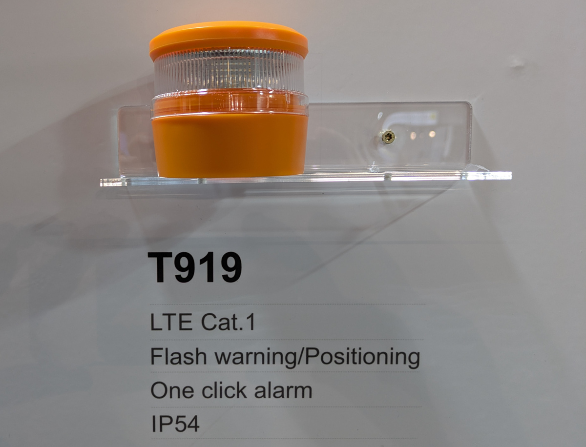  ### Kostenloses, ad 1 – Renesas Am Stand von Renesas gibt es – bei qualifizierter Anfrage – Evaluationsboards mit dem neuen RA0E3-Koprozessor. 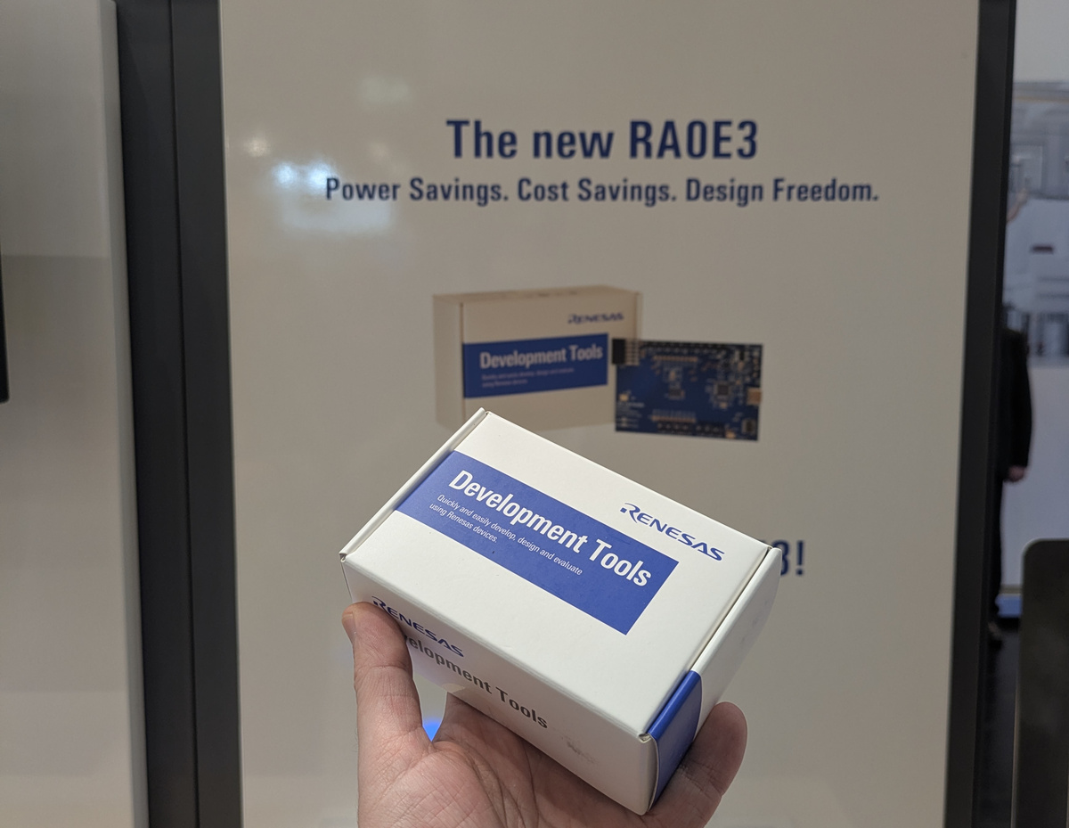 ### Kostenloses, ad 2 – nur noch Freibier
Martin M. schrieb im Beitrag #8021858: > Hallo Tam, vielen Dank für deinen Messbericht! > Könntest du noch das/die Bild(er) von "QuecTel, ad 2 – vom Funkmodul" > ergänzen? Danke! Hallo, sorry für die
LA32) ilp32d abi and LoongArch32 Reduced(LA32R) ilp32s abi. The ilp32 abi is similar to lp64 abi[1], with some differences in details. Most gcc testcasese has passed when using qemu-user. A LA32 linux system based on qemu is here[2]. The binutils and glibc sources is here[3] [4]. A LA32 instruction
any LA64 manual. A Chinese LA32R instruction set manual is here[6]. [/c] ### CircuitPython 10.1.0-beta.1 mit Unterstützung für MIPI DSI-Display MIPI DSI-Displays sind für die Übertragung „größerer“ Informationsmengen ideal. Mit dem ESP32-P4 steht bald eine Implementierung ante Portas, die im Maker-Bereich
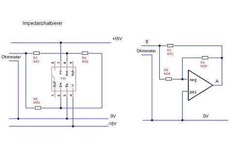
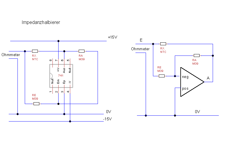
NC Ne —s m izquiere IN —2 7 n-Q Oesire v- —s snm INe—p 6 reşire Q NC. —7 sc. Lai 5 Onu v-a k slnu 4 BA 741J741 I]7A1 MBA 7415741 JH/741 MH GA 741 N/741 IN/741 MN 12 BA 741/741)/741M ABSOLUTE GRENZWERTE e Versorgungsspannung
- G C A D G t d h 0 r l S / h r l r e i l a B / - i 6 o 0 - a o 0 O L p C R a o i 1 e e U 2 C P F P M H F D ( I 8 T 1 C 1 5 C C 1 C C O Z P D M H ( P S E I PIC16(L)F1764 1 7 4 128 512 12 1/3 3 2 8 1/1 1 1/1 1 3 1 1 1 1 2 ü 1 1 PIC16(L)F1765 1 14 8 128 1K 12 1/3 3 2 8 1/1 1 1/1 1 3 1
current 0.01 50 mA withstanding voltage for 1 minute 250 Vac contact resistance applying load of 2 times operating force at 5 Vdc, 10 mA 100 mΩ insulation resistance at 100 Vdc for 1 minute 100 MΩ operating force see
Capacitancetolerance -10 +30% i APPROVALS: e RatedvoltagerangeU 16…450V a • RoHS compliant n SurgevoltageU U ≤315V:U =1,15U ;U >315V:U =1,10U c S R S R R S R n Max.reversevoltage 2V • REACH compliant t m o Categorytemperaturerange -40°C...+85°C i n LeakagecurrentI afLer5min@U R ≤0,008*C [µFR*U [V]+6RA[µA] , c Usefullife3000h
Capacitancetolerance -10 +30% i APPROVALS: e RatedvoltagerangeU 16…450V a • RoHS compliant n SurgevoltageU U ≤315V:U =1,15U ;U >315V:U =1,10U c S R S R R S R n Max.reversevoltage 2V • REACH compliant t m o Categorytemperaturerange -40°C...+85°C i n LeakagecurrentI afLer5min@U R ≤0,008*C [µFR*U [V]+6RA[µA] , c Usefullife3000h
Jetson AGX Xavier Developer Kit Jetson Xavier NX Developer Kit Jetson TX2 Developer Kit Jetson TX1 Developer Kit Jetson Nano Developer Kit Jetson Nano 2GB Developer Kit Jetson TK1 Developer Kit [/c] ### OrangePi Zero 4 steht unmittelbar bevor Im Bereich der kompakten Prozessrechner aus
inspection devices, smart intercoms, safety equipment and multimedia applications. It integrates LTE Cat 4, Wi-Fi 802.11ac, Bluetooth 5.1 and GNSS in a compact LCC form factor and supports a wide range of interfaces for rapid integration. SE505FE: Android 16 5G smart module for next generation connected
N N N N N N N N N N N N N N N N N N GND G G G G G G G G G G G G G G G G G G G G G G G G G G G G G 4 5 6 7 8 9 0 1 2 3 4 8 9 0 1 4 8 9 0 9 1 0 9 0 3 4 5 6 7 G G G G G H H H H H H H J J J K K K K L L L M 1 1 1 1 1 1 M M M M M M MSD93F1TW2 Chassisplatte / Chassis Board – IR/Keyboard (+) 1 2 +5V2_ST KEYPAD
a e n d e d e 22p e e e S 10k r S A r o 6 8 0 O o 8 E O m 470k m A e 240k 47u 6 8 0 b e b t k 470k 0 k 1n e t C e N 1 47k r N 4 4 LM4040 r . 47u k k 10k 10k 10k e . 0 S e 2 4,7 uH 330k 1 8 3 R 1M e P BSS84 R7 e k 2 6 2 ( B 5 ( T 9 T e e 10k l l 2 1 ) M ) U
R 6 = R 7 = R 4 = R 5 dann ist U a = U e2 - U e1 oder b) wenn die Widerstandsverhältnisse gleich sind : R 6 \R 4 = R 7 \R 5 Dann ergibt sich für Ua: U a = (U e2 R 7 \R 5 ) - (U e1 R 6 \R 4 ) oder noch einfacher: U a
R4 und Rc Variablen für Zustand 1 eingesetzt, bildet 1. Gleichung Variablen für Zustand 2 eingesetzt, bildet 2. Gleichung 2 Gleichungen mit 2 Unbekannten, Lösung durch Umformen der 1. Gleichung nach R4
Kontokt 6 Die Stromaufnahme beträgt bei ei.ngelegter Cassette am Bandanfang: \ bei Uiedergabe ohne 5igna1, max. 25 mA bei Aufnahme ohne Signal, max.45 mA. Kontokt 9 Bei zu hoher Stromaufnahme ist dle Leichtgängig- keit der [v]echanik zu überprülen. 4 08 r9 t6 t2 t-.4 r8t 0,rl R30 L J l^ D6l7 965r -28?.q?
e [ e u N - C S O i D c r R u0.6 D 0 S r10 n v r R 150℃ 25℃ D0.3 ,R ※Notes: ID 1.VGS0V ※ Note:T =25 2.250 sPulseTest J 0.0 10-1 0 10 20 30 40 50 60 0.2 0.4 0.6 0.8 1.0 1.2 1.4 1.6 ID,DrainCurrent[A] VSDSource-Drainvoltage[V] Figure 3. On-Resistance Variation vs Figure 4. Body Diode
.' REM l 7'J R E H a u p tp ro q ra m m ISO REM 19O XO FF=4O U :YO FF=2S5 2OO XFAF T=3O O : YFflf T = lf!O 2U> FD P K - oTD 1.2 STEP .(.)?. 2 2 0X l=h : V l = f :64 / D 2 "O NEXT r- 2 4 0F O R 1 =T D .7 STEP - . o J 25O X l = t * . 6 :
h l Torsteuerung i nB e t r i e b Tore•Türen• Antriebe n e h m e n 1 9 2 3 4 ELEKTRONIK 2500 DIGITAL RADIO CONTROL TELECOMMANE BEREIT POWER ALIMENTATION | | O ) ( U a> 8 3 o UJ 3 E ü t y "o o ® O O M I —.) M^ i 1 — 1 —r— 1 ' 2 fTuj o> rztiJ ® O O ^ u0) O O ai q
............... B C S 4 8 C R 23 .................50 01, Poti, O n, 4 I so! cr01 ppcl dai u T 2 - T 5 .......................1 0 1 4 2 6 mm Achse I Schraube M 3 x 6 miii F 7 r I p R 24 100 kIl 4 Schrauhen M 3 x 16 111111 I) I - D 8 ........... L L I), rot, 501111 R 77 I MI) 5 Muttern M 3 1)91)11) 1)19 D21) DII) 1N4001 R14 2201 4 Schrauben M 4 x 55 rnmi D II - 1) 14 ................R 250 13 R 19 - R 4' I I) I W 12 Muttern M 4 1) IS - I) 18, D 21 - D 29 I N4148 R 44 R 50 3,3 0) Digitales
CMOS Logic “0” voltage1) VOL I 0.6 V Logic “1” voltage1) VOH I 2.4 V Note: 1. With IOL= 1 mA and IOH = -1 mA 7 5364A–BIOM–11/03 . Table 8. Switching Performances The following characteristics are applicable to the operating
MHz - mit NPU Wireless Familie, mit integrierten Funk-Schnittstellen STM32WL (2019) ARM Cortex M0+ und M4F bis 48 MHz sub-GHz z.B. für LoRaWAN, Sigfox, W-MBUS, Mioty, Wi-Sun, IEEE 802.15.4g STM32WB0 (2024) ARM Cortex M0+ bis 64 MHz 2.4 GHz mit Bluetooth 5.4 STM32WB (2018) ARM Cortex M0+ und M4F
typischer Features auf STM32 Mikrocontrollern. Nicht jede Serie hat alle Features. ARM Kerne Cortex-M0(+): 0,96 DMIPS pro MHz Cortex-M3: 1,25 DMIPS pro MHz Cortex-M4F: 1,25 DMIPS pro MHz, mit FPU Cortex-M7F: 2,14 DMIPS pro MHz, mit FPU Cortex-M33F: 1,5 DMIPS pro MHz, mit FPU Cortex-M55F: 1,69 DMIPS pro
CMOS (1) Logic “0” voltage VOL I 0.6 V (1) Logic “1” voltage VOH I 2.4 V Note: 1. With I = 1 mA and I = -1 mA OL OH 7 2150B–BIOM–09/03 Table 6. 5 V Power Supply The following characteristics are applicable to
GSS Gate to source leak current Vgs=10V, V DS=0V - - 5 uA VTH Gate threshold voltage Vds=12V, IDS=1mA 1.6 2.0 2.4 V Pout Output power f=175MHz ,Vds=12.5V 70 75 - W D Drain efficiency Pin=4W, Idq=2.0A 55 60 - % Pout Output power f=520MHz ,Vds=12.5V 50 55 - W D Drain efficiency Pin=10W, Idq=2.0A 50 55
1 50m L1 = 2πf × 2 + XC m + 1 1 50 × 1.508 L1 = 2π × 868MHz × 2 + 1.27 = 4.45 nH 1.508 + 1 The result on the Smith chart is shown in the figure below. Figure 30. L1 used to match the RF PA reactive part
by the the required non-standard $ IEEE 754 data type conversions three components named mantissa (M), exponent (E) and into scheduled CDFGs. Section 4 experimentally evaluates E▯b S out approach by comparing it to current academic and sign (S), s.t. R = M ▯ 2 ▯ (▯1) where the bias b is a positive integer
! R ! ! R 1 ! 0 R D C C C T C C 0 2 2 1 4 3 4 1 2 9 N 5 O GND E1 M T X2 9 - V . . C 1 3 4 C5 V 4 N B 2 0 0 M N 2 2 1 1 1 C E 9 M X . R 1 R 1 O CN63 T CHGND 1 EN 3 LF91 2 OC 6 CVA30180J 3 6 N 3 -DATA N B 4 +DATA
. Zahlung per Rechnung, Bankeinzug nur für Stammkunden (ab 4 bis 5 Bestellung), Für Institute/Firmen direkt auf Rechnung möglich Abholung von Ware in Bonn-Tannebusch möglich Umzug ab 1.1. 2024 nach Bonn Tannenbusch. dad24. Homepage, Shop: E-Bay Shop: nicht mehr
Walter Computer Technology" kleines Lieferprogramm aber ein paar interessante Produkte SMG Diffusion - F1GE. Homepage: ( Seite nur französisch ) Videotechnik, 1,2 GHz / 2,4GHz Module Gebraucht-Messgeräte HP, Tek, Philips u.a. GHz-Halbleiter Koax-Adapter Antennen SOL-EXPERT / Edunikum. Homepage: Bausätze
t , e ੌ m ਃ c ష D e i i B a T S D 1 3 5 2 4 6 8 1 1 1 1 1 2 1 3 5 7 9 1 1 1 A A A A A A A A A A D D D D D D D D M M M M M M M M M M M M M M M M M M ) D 0 D 2 4 6 8 0 2 4 6 8 0 2 4 6 8 0 2 4 6 8 0 0 1 1 1 1 1 2
L T G . 5 L . 5 4 4 1 . 0 1 7 . 7 1 5 4 L S 7 4 D M F L I P F L O P L 1 4 3 D R O S S E L 5 L . 5 0 5 3 . 0 0 5 . 9 4 M H 1 + - 1 0 X 0 , 0 2 8 A 7 2 O H M T Y P M S 7 5 0 8 5 - 1 9 L 4 4 D R O S S E L 5 L . 5 0 5 3 . 0 0 3 . 3 1 U H 4 7 + - 1 0 X 0 , 1 1 A 4 , 5 O H M T Y P M S 7 5 0 8 5 - 3 L 4 5 4 6 D R O S S E L 5 L . 5 0 5 3 . 0 0 5 . 9 4 M H 1 + - 1 0 X 0 , 0 2 8 A 7 2 O H M T Y P M S 7 5 0 8 5 - 1 9 R 1 4 3 S C H I C H
52 29R 5 5 3 61 GES 06 42 19R R R L 81 GES 26 22 38R k7. 4 05R 2 91 GES 36 12 1TNI L 02 GES6 02 18R k7. 4 15R 0 1 2 3 4 5 6 7 8 9 L 1 2 3 4 5 6 7 1 1 1 1 1 1 1 1 1 1 2 2 2M M M MS N U0 1 2 S E LT B A E E EC C C C VX XK K K T E HI e S S S R 0 1 5 d - - 5 5 W
52 29R 5 5 3 61 GES 06 42 19R R R L 81 GES 26 22 38R k7. 4 05R 2 91 GES 36 12 1TNI L 02 GES6 02 18R k7. 4 15R 0 1 2 3 4 5 6 7 8 9 L 1 2 3 4 5 6 7 1 1 1 1 1 1 1 1 1 1 2 2 2M M M MS N U0 1 2 S E LT B A E E EC C C C VX XK K K T E HI e S S S R 0 1 5 d - - 5 5 W
mechanism of the Hitag2 D0 41 FB B8 01 3B 54 10 protocol apart from the cryptographic algorithm. Be- 25 1A 3C AD 15 88 5E 19 05 7A 9C 8D F7 4D F7 70 sides the fact that the transponder proves knowledge of C5 3A 5C 4D 30 B1 4A D4 the secret key,it sends its passwordencrypted. In general E5 DA FC 6D D8 BD
xxxxxxxxxxxxxxxxxxxxxxxxxxxxxx xxxxx xxxxxxxxxxxxxxxxxxxxxxxxxxxxxxxxxxxxxxxxxxxxxxxxxx xxxxxxxx C P M xxxxxxxxxxxxxxxxxxxxxxxxx xxxxxxxxxxxxxxxxxxxx xxx N O r R M d 5 X P u 2 P N t S Y a ADDRESS DATA e P a m U s RX L e SA A0 A1 A2 A3 A4 A5 (1)R/W SO SA D0 D1 D2 D3 D4 D5 D6 D7 SO c C e o t n d u c o r ADDRESS s TX SA A0 A1 A2 A3 A4 A5 (1) R/W SO l f m o R p e v . d MX . n — s 1 o DTRQ 1 7 m 001aak589 9 A n S p s a l b (1) Reserved. n 2 c d 1 o Fig 10. UART write data timing diagram a 6 g d d p l Remark: The data byte can
the selection of all Y deflection coefficients from 1 a phase difference of 180° and enters the External Trigger mV/cm to 20 V/cm. Channel Switch. 1.1.4 Variable Gain and Symmetry 1.2.4 Trigger Source Selection In the next stage (VAR. GAIN) the fixed Y deflection

 Bild
Bild
 Bild
Bild