or receive in MDIX mode 44 P0_RX+ I/O Port 0 TP RX 45 P0_RX - These two pins are the Twisted Pair receive in MDI mode or transmit in MDIX mode 47 BGRES I/O Band-Gap Pin Connect a 6.8K±1% ohm resistor to BGGND in application 48 BGGND
to 48 kHz (two channels, 64 times oversampling on each channel) High Bandwidth Mode 192 kHz THD + N measurement High Bandwidth Mode Residual THD + N THD + N measured using the high bandwidth ADC over an 80 kHz BW. The measurement is noise-limited for amplitudes below 125 mV (–16 dBu). Input > 125 mV
bei 80 Grad ist die Grenze für die firmware Lüftung. Hab es so justiert dass es nicht über 60(meist) 65(manchmal) 70(fast nie) grad geht. Mit CoreCTL und MSI Afterburner.
https://www.overclockers.ua/video/asus-rx550-4g/all/ Fotos hab ich hier gefunden, also für mich ist da genug Abstand, und die ram klötze sind ja aus kunststoff. Das ist sie da sieht man auch die Folie: https://ru.gecid.com/news/videokarta_asus_phoenix_radeon_rx
63 AD0 P_PMON_10 I Sense Power Loading <Variant Name> 64 AD1 BAT_IN I sense Battery EC Pin Define 65 AD2 N.C I Reserved Title : 66 AD3 N.C I Reserved ASUSTek Computer INC. Engineer: Kell_Huang Size Project Name 68 GPO3C DOC O Trigger Clock Gen Rev http://hobi-elektronika.net A3 P701 1.2G DateFriday,
KEEPALIVE mechanism CH9121 Datasheet 2 3. Package 6 6 6 6 6 5 5 5 5 5 5 5 5 5 5 4 8 0 1 1 2 2 8 # # 1 C C N N G E D D D D C K T I N N C C C E T R XTXR C I A D 1 V V R V L 48 2 RSETE GND 47 3 VCC33 NC 46 4 GND DIR2 45 RXP VCC33 5 RXN GND 44 6 VCC18 VCC18 43 7 TXP VCC33 42 8 TXN GND 41 9 GND VCC33 40 10 XI NC
The circuit that converts a balanced circuit into an unbalanced circuit is called BALUN. Thus, the Rx matching network also plays the BALUN role. AN5457 - Rev 3 page 16/75 AN5457 Receiver Figure 19. Diagram of Rx circuit with load RFO_HP RFO_LP RF switch STM32WL RFI_P Rx input matching Load RFI_N network
R, L, H models 3 RX-V4A/TSR-400 T model B, G, F models K model V model A model P, S models 4 RX-V4A/TSR-400 n REMOTE CONTROL PANEL TSR-400 G model RAV574 T model 5 RX-V4A/TSR-400 n SPECIFICATIONS n Audio Section Frequency
workstation slave 1 number ① C P T 4 = C P T 4 + 1 YES function code NO not known exception YES length NO n° 1 incorrect CPT3 = CPT3 + 1 exception n° 3 YES addressing NO CPT3 = CPT3 + 1 incorrect exception YES data NO n° 2 incorrect CPT3 = CPT3 + 1 exception n° 3 2 CPT3 = CPT3 + 1 Modbus.org http://www.modbus.org
R712 7 R720 Q681 0 1 4.USBD+ C C 4.USBD+ 3 R721 5.DGND 1 1 5.DGND . . . . . 2 S S S L L G G V V V N N V V V N N 3 3 0 0 R R D D S S S 2 C . . . . . C C C C 6 6 W W W 1 2 3 4 5 BasicConnector R663 9 2 AC INLET (A SIDE) AC INLET (B SIDE) CN90 9 X L FH92 C L RX92 RX91 CUP12674Z-3 MP VT91 V 3 0 Y 9 0 2
Bestückungsplan ist zu sehen (Screenshots anbei), Im Bestückungsplan steht 40 Wdg. Mit Al = L / N^2, ergibt das Al = 2875 nH/Wdg^2. Auf dem Foto zähle ich allerdings 41 Wdg. und damit AL = 2736 nH / Wdg^2. Ziemlich dicht dran an H. H. schrieb im Beitrag #8027306: > Das klingt doch sehr nach TDK/Epcos/Siemens R17 aus N30. AL / nH = 2710 +/-25%
time different between two active clock edges td0 = 0ns. By doing this, we will know that at time tpN = N * LCM(PL, PR), the 2 clocks’ active edge will be aligned again. Here N is any integer, and LCM is “least common multiple”. For example, if PL is equal to 2 and PR is equal to 3, then LCM(PL, PR)
Ein Hinweis waere, die Spule mit Anzapfung so waehlen, dass man den Tastverhaeltnisbereich 35...65% nicht verlassen muss.
eingebaut, die ich tatsächlich einfach nur rumliegen hatte, allerdings mit besserer Gate Charge (SUP75N05-06, Qg=85nC, vorher IRFB3077, Qg=160nC), Wirkungsgrad bei 500W etwa 2,5% besser. Also ist die Treiberstufe immer noch scheiße, aber sie kommt mit FETs mit geringerer Gate-Charge deutlich besser klar
m o . n o x l - n n a m r l o n . t w l E w E w F 1 - _ 7 0 2 Electrical Diagrams and Operation Manual BK150FUE-1 SMART START™ NXT SINGLE PHASE CONTROL BOX For professional installers only Keep this document
: TPA3255 2 Page: Audio in AB P k 0 3 e 4 0 5 F V } R 5 W 5 N X X Z 2X5R b 44 4b2N CC2 C 2 C 1 R R%52 N INPUT_A BST_A 2 5 1 3 1RX 1 5 1 C 10nF R100,0k C 33nF C23 2 100V R7 7 0805 C25 2 100V Audio in CD 1 3 0805 2 125mW 5 0805 X4-a$65 X4XZ4 2X2C 2Z7R 2X2C L 2 Z
loads such as coils and motors. — Using MOS technology to design power tube The circuit integrates N-channel and P-channel power MOSFETs. — 1 channel 1.6A power tube internal resistance 0.4 ohm The voltage range covers 2V to 8.6V. 27ÿ, VDD=6.5V, two — 2 channels 1.6A power tube internal resistance 0.4
Vielen Dank für eure Antworten. Also laut dem Internet zieht der ESP32-C6 im Worst-Case: Empfang (RX) • 802.11b/g/n, HT20: ca. 70–80 mA Senden (TX) • bei 0 dBm Ausgangsleistung: ca. 60–80 mA • bei +11 dBm Ausgangsleistung: ca. 110–130 mA • bei +20 dBm (Maximalpegel): ca. 220–260 mA Verbunden,
Gerd E. schrieb im Beitrag #7907813: > 6+n Gar nicht!
USB data transmission, and RB_UEP_AUTO_TOG=1 is set to realize automatic switch. Table 16-4 Endpoint n buffer modes (n=1/2/3) RB_UEPn RB_UEPn RB_UEPn_ _RX_EN _TX_EN BUF_MOD Description:Arrange from low to high with R16_UEPn_DMAas the start address 0 0 X Endpoint is disabled, and R16_UEPn_DMAbuffer is
The circuit that converts a balanced circuit into an unbalanced circuit is called BALUN. Thus, the Rx matching network also plays the BALUN role. AN5457 - Rev 3 page 16/75 AN5457 Receiver Figure 19. Diagram of Rx circuit with load RFO_HP RFO_LP RF switch STM32WL RFI_P Rx input matching Load RFI_N network
.................................................................................................. 65 Changing from desktop to tower orientation ..................................................................................................... 66 vi 5 ComputerSetup(F10)Utility.....................
13293-306. IRWIN , G.R. [1964]: Structural aspects of brittle fracture. Applied Materials Research 3, 65-81. K UNA ,M. [2010]: Numerische Beanspruchungsanalyse von Rissen, 2. Aufl., Vieweg + Teubner. M USCHELISHWILI , N.I. [1971]: Einige Grundaufgaben zur mathematischen Elastizitätstheorie. Hanser, München
in Bild 34c dargestellten Schaltung liegt die Netzspannung anfangs über einen Widerstand (20 bis 30 n 5 Relaisschaltungen 65 0) Si , C rD J c - ~ ,,"'t ~ R ~ f -- -- -- - _ - < C J b) 209 c) Bild 3-b) Alarm bei defekter Sicherung, c) Unterdrückuug dcr'Einschaltstrom· spitze bei NctztransfonnatorcIl 10
active-low output from the CP2110 and indicates to the external UART device that the CP2110’s UART RX FIFO has not reached the watermark level of 450 bytes and is ready to accept more data. When the amount of data in the RX FIFO reaches the watermark, the CP2110 pulls RTS high to indicate to the external
9 9 w w 4 ı 23288 ]C3223E > 3KO2 HFHBBQG N w n t I§I 1 86 792 2 3 2 Ø B h J3222 23122« o MÜLEX65 231222I 1523277 52R2 221K52__3 56R32 T3EF 12V t oíoı zv 1 23SKGZ n 2vz1 23BH3+¬2 o n < t Boflrd Bvzz > c < c 7 2 4 2492 232222 1222 1 7 e m 0-5--O-SV
State-Machines. Somit sind viele von Hause aus recht Stromsparend. Der PCA9554 benötigt z.B. nur 250nA im "Standby-Mode" (keine Kommunikation). Bei I2C gibt der Master den Takt (SCL) für die Datenübertragung vor. Die Slaves benötigen im Gegensatz zu UART also keinen genauen Taktgeber (Quarz). Will man
zu "tunneln" (PHY Layer). Dabei werden die TX und RX Leitungen des I2C Bustreibers mit den TX und RX Leitungen des RS-485 oder CAN Treibers verbunden. Für SDA und SCL werden hierfür auf dem Übertragungskabel also insgesamt vier Leitungen benötigt. NXP
active-low output from the CP2110 and indicates to the external UART device that the CP2110’s UART RX FIFO has not reached the watermark level of 450 bytes and is ready to accept more data. When the amount of data in the RX FIFO reaches the watermark, the CP2110 pulls RTS high to indicate to the external
Peter K. schrieb im Beitrag #7854254: > rxw RX... sind bei Rubycon Hochtemperaturelkos, für mehr als 105°C spezifiziert.
Nachtrag: - das Brikett funktioniert wieder - Ursache für den Defekt des Elkos waren C2/C3 statt 680nF hatten die noch 400nf und 0,56nF; dadurch lief die Spannung am Elko auf über 560V hoch (Leerlauf, hab bei 560V abgebrochen); gleicher Effekt wie bei den LG-Netzteilen im Standby (die mit den üblen

 Bild
Bild
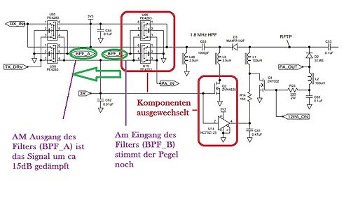
 Bild
Bild
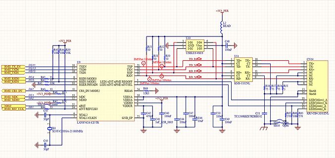
 Bild
Bild
 Bild
Bild
 Bild
Bild