(62.214.0.77) 5.271 ms 5.128 ms 5.429 ms 4 62.214.73.216 (62.214.73.216) 5.481 ms 5.408 ms 5.405 ms 5 62.214.73.217 (62.214.73.217) 15.268 ms 22.199 ms 20.350 ms 6 172.67.70.44 (172.67.70.44) 5.883 ms 5.853 ms 6.097 ms admin@iMac27-Frank-Home
Adresse am Ende. Ach Herr jeh, bei Versatel ist das wohl dann so die Norm? ;-) Bei mir kommen da max. 310 m-sec. zusammen, was schon das Einfache über dem zulässigen Limit von max 150 ms wäre!
angle • 4.3~15.3 mm actuator • through hole SPECIFICATIONS parameter conditions/description min typ max units rated voltage 1 12 Vdc rated current 0.01 50 mA withstanding voltage for 1 minute 250 Vac contact resistance applying load of 2 times operating force at 5 Vdc, 10 mA 100 mΩ insulation resistance
nach ISA""" # Vereinfachtes Modell der Temperaturschichten if h > 20000: # Stratosphäre Teil 2 T = 216.65 + (h - 20000) * 0.001 elif h > 11000: # Stratosphäre Teil 1 (Isotherm) T = 216.65 else: # Troposphäre T = 288.15 - h * 0.0065 rho = rho0 * np.exp(-g * h / (R_spec * T)) # Barometrische Höhenformel
Zigbee2Mqtt das Joinen aktiviert. Natürlich ist der Abstand zwischen ESP und Zigbee Stick gering (max. 1m, direkte Sicht). Und falls es irgendwie hilfreich ist: Z2M nutzt den Kanal 11. Ich habe den ESP mehrfach mit idf.py erase-flash flash monitor nach bestem Wissen neu aufgesetzt. Und im Monitor
/O pins I (214) cpu_start: Pro cpu start user code I (214) cpu_start: cpu freq: 160000000 Hz I (216) app_init: Application information: I (220) app_init: Project name: powermeter I (224) app_init: App version: 277ad0a I (228) app_init: Compile time: Mar 6 2026 21:44:18 I (233) app_init
- RICHTIG - Optokoppler isoliert. Sollten mal versehentlich 230V auf die Eingänge kommen , sterben max. die Optokoppler. Und Dein sensibles Zeugs überlebt es. Also : Eingänge mit Optokoppler Die Schaltung innerhalb der Optos vernünftig aufbauen. Ausgänge mit Relais und Freilaufdioden. Also erzähl
www.schloeder-emv.de/fileadmin/schloeder-emv/deutsch/EMV_Pruef-_und_Messtechnik/ESD-Simulatoren/DB_SESD_216.pdf > > Die Anstiegsflanke des hohen Peak dauert unter 1ns. Der langsame Peak > kommt nach 20ns, nur um dir eine Vorstellung zu geben, wie die > Anforderungen sind. Ah - hochinteressant!
aus der nachstehenden For details please refer to the following checklist: Bandbreite: min. 10 mm max. 400 mm Strip width: min. 10 mm max. 400 mm Checkliste: Streifenlänge: min. 20 mm max. 3000 mm Strip length: min. 20 mm max. 3000 mm Lochdurchmesser min. 4,5 max. 28 mm Hole diameter: min. 4.5 mm max. 28 mm Bandbreite: min. 10 mm max. 400 mm Strip width: min. 10 mm max. 400 mm AnzahStreifenlänge: enen Lmin. 20 mm ser: max. 3000 mmmax. 3 NumbStrip length: t diamemin. 20 mm max. 3000 mm max. 3 Materialstärke 0,27 / 0,30 / 0,35 / 0,50
= 25℃; the others floating unless otherwise specified. Parameters Symbol Test Condition Min. Typ. Max. Unit Input operation voltage Vin 8 36 V Quiescent Supply Current I V =Vin 2.1 5 mA q FB Oscillator Frequency Fosc 144 180 216 KHz Output Short Frequency Fosp 48 KHz Switch Current Limit IL VFB =0 7 A Max. Duty Cycle D MAX V FBV 100 % VFB0V, Vin=12V, moh Output Power PMOS Rdson SW=5A 60 80 m Rev 1.5 www.xlsemi.com 5 Datasheet 5A 180KHz 36V Buck DC to DC Converter XL4015 Typical SystemApplication (VOUT
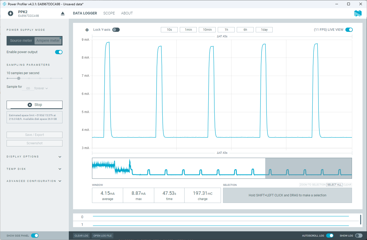
SAMPLE PARAMETERS 10 samples per second Sample for forever Stop Estimated space limit ~5193d 15:37h at 216.0 kB/h. Available disk space 26.9 GB Save / Export Screenshot DISPLAY OPTIONS TEMP DISK ADVANCED CONFIGURATION WINDOW SELECTION ZOOM TO SELECTION SELECT ALL CLEAR 4.15mA average 8.87mA max 47.53s time
7016 KEY FEATURES Befestigungslöcher im Gehäuseboden vorhanden Load-carrying capacity 25 kg per foot, max case weight: 50 kg PRODUKTMERKMALE Produkttyp: Gehäusefuß, 45mm hoch Typ: Gehäusefuß, 45mm hoch Passend zu: Gehäuse Anzahl pro Packung: 4 ZUSÄTZLICHE PRODUKTDETAILS Flexibler und robuster Aufstellfuß
zusammen benutzen kann. https://www.techpowerup.com/gpu-specs/tesla-m10.c3035 Der AMD Ryzen™ AI Max+ PRO 395 macht so um die 200GB/s auf dem Speicher und man kann eben 128GB RAM reinmachen. Allerdings kostet so ein komplett neues System natürlich auch sehr viel mehr als 200€ für eine M10.
Qwen3-coder-next 80B sollte eigentlich komfortabel auf deinen RTX-Stack passen. Achte auf ein max. Kontextfenster. Viel Spass beim Agent-Tuning ;)
---------------------- --------------- V IN(min)– Vsat V IN(min)– Vsat – VOUT V IN – Vsat (t + t ) max 1/f 1/f 1/f on off min min min C 4.5x10 t5 4.5x10 t5 4.5x10 t5 T on on on I 2I [(t /t )+1] 2I 2I [(t /t )+1] PK(switch) out(max) on off out(max) out(max) on off R 0.3/I 0.3/I 0.3/I SC PK(switch) PK(
+25°C. Boldface specifications apply over the T range of -40 C to +85 C. A Parameters Sym Min Typ Max Units Conditions PMOS Switch ON Resistance RDS(ON)P — 0.9 — V IN= 3.3V,SW = 100 mA NMOS Peak Switch Current N(MAX) 600 850 — mA Note 5 Limit V Accuracy V % -3 — +3 % Includes Line and Load OUT OUT
Cortex M4F bis 180 MHz STM32H5 (2023) ARM Cortex M33F bis 250 MHz STM32F7 (2016) ARM Cortex M7F bis 216 MHz STM32H7 (2018) ARM Cortex M7F bis 400 MHz STM32N6 (2025) ARM Cortex M55F bis 800 MHz - mit NPU Wireless Familie, mit integrierten Funk-Schnittstellen STM32WL (2019) ARM Cortex M0+ und M4F bis 48
auf Debugging von max. 32KB Code limitiert, keine Limitierung beim Complilieren) Rowley Crossworks (Demo 30 Tage unbeschränkt, 150$ für nichtkommerzielle Nutzung, auf GCC basierend). Mir ist nicht klar warum man für diese
0 V; Tamb = 40 C to +85 C; unless otherwise specified. [1] Symbol Parameter Conditions Min Typ Max Unit Supplies V DD supply voltage 2.3 - 5.5 V IDD supply current operating mode; V DD = 5.5 V; no load; - 350 550 A V = V or V ; f = 100 kHz I DD SS SCL Istb standby current Standby mode; V DD = 5.5
25°C(Note2). V =V =EN =EN =10V, MODE=0V, R =200kΩ A IN_P IN_N T SYMBOL PARAMETER CONDITIONS MIN TYP MAX UNITS Boost Charge Pump VIN_P VIN_PInput Voltage Range l 4.5 16 V VUVLO VIN_PUndervoltage Lockout Threshold VIN_PRising l 3.8 4 V VIN_PFalling l 3.4 3.6 V I V Quiescent Current Shutdown, EN = EN = 0V
Recommendations Following is the recommendation for manual 300 soldering with a soldering iron. 260°C 2+3seconds max 250 First Wave Second Wave Recommended Soldering Temperature 400 )00 ( ∆ T < 150°C 350 r Cooling t C r50 Preheating ca. 2°C/second e 300 p ca. 3.5°C/second typical t e ca. 5°C/second e 250 100 T preheat
0°C to +70°C Industrial(I):Tamb = -40°C to BSEL = 0 BSEL = 1 +85°C Symbol Characteristic Min Typ. Max. Min. Typ. Max. Units TE Basic pulse element 260 400 620 130 200 310 μs TBP PWM bit pulse width 3 3 TE TP Preamble duration 28 28 TE TS Sync Pulse duration 10 10 TE TH Header duration 10 10 TE THOP
H2 I H 1 L 0 - 40 0 55 85 125 150 P d Tamb(°C) Note • Zero power is considered as measuring power max. 1 % of max. power. PHYSICAL DIMENSIONS FOR RELEVANT TYPE (all dimensions in millimeters) H1 R25VALUE BMAX. d H2 MAX. L P T MAX. MIN. MAX. 3.3 to 220 5.0 0.6 ± 0.06 1.0 4.0 6.0 24 ± 1.5 2.54 4.0
H2 I H 1 L 0 - 40 0 55 85 125 150 P d Tamb(°C) Note • Zero power is considered as measuring power max. 1 % of max. power. PHYSICAL DIMENSIONS FOR RELEVANT TYPE (all dimensions in millimeters) H1 R25VALUE BMAX. d H2 MAX. L P T MAX. MIN. MAX. 3.3 to 220 5.0 0.6 ± 0.06 1.0 4.0 6.0 24 ± 1.5 2.54 4.0
The thermistor is used to Table 2. NTC THRMISTOR SPECIFICATION Parameter Symbol Condition Min. Typ. Max. Unit Resistance R 25 TC= 25°C 99 100 101 kW Resistance R100 TC= 100°C 5.18 5.41 5.60 kW Temperature Range −40 +125 °C ] [ e l V e n t s e r t i r h T Case Temperature [5C] Figure 8. NTC Thermistor
character generator ROM (code 0101) T6963C−0101 is built in as standard. ▯External display memory : 64 KB Max The addresses in display memory of the text area, graphic area and external character generator area are determined by software. ▯Read or Write operations from the CPU do not disturb the display. ▯A
button “zero set on/off” 1.6. D C C U R R E N T M E A S U R E M E N T S Ranges :20mA,20mA,2.4,208 (max, input current in highest range) #10 A (20 A for max, 20 sec.) Resolution 510HAin20mArange Number of representation units £2200 Acuracy ++(0.5%ofreading+0.1%offulscale) Temperature coefficient +0.05%
LED source.This equation can be simplified further by replacing the K2/K1 ratio with BIN Typ. Min. Max. IL300’s transfer gain, K3. A 0.59 0.56 0.623 Equation 22:Vout/Vin=– K3 • (R2/R1) B 0.66 0.623 0.693 The IL300 isolation amplifier gain stability and offset drift depends on the transfer gain characteristics
▯ } I ( ▯ 2 › 2 LED Driver IC ▯ D O ▯ î C ▯ +12V_FAN LED Forward Voltage E 2 2 1 1 SDICS ▯ +15V R_Max 2.4V x 4 pcs = 9.6V L L L L SDI_CLKL ) For EMI ▯ 3 3 3 2 2 2 1 1 1 G_Max 3.3V x 4 pcs = 13.2V C227 C100p50N0402 LED1_G L L L L L L L L L Pin Definerd 6 5 4 3 2 1 O ▯ C567 C100p50N04N2 LED1_R B_Max 3.3V
Save-Schaltfläche. Die automatische Helligkeitssteuerung verwendet dann bei einer Helligkeitsmessung diese Min-/Max-Werte zum Vergleich. Somit kann der Helligkeitsbereich bei der automatischen Helligkeitssteuerung komplett ausgenutzt werden. Hinweis: Es ist nicht sinnvoll, bei der Max-Messung einfach eine Taschenlampe
bestimmten Anzeigemodi. Bugfix SK6812: Rot und Grün vertauscht. Bugfix LDR: Nach dem Setzen eines neuen LDR-Max-Wertes wurde dieser nicht zurück an das Web-Interface übertragen und deshalb dort (bis zum nächsten Reboot) ein alter Max-Wert angezeigt. STM32 Version 2.1.0. Auslagerung des HTML-Codegenerators auf
portEthernetSwitchControllerwithMII/RMIIInterface 10.4.4 Port 2 RMII Interface Transmit Timing Symbol Parameter Min. Typ. Max. Unit T1 RMII REF_CLK Period - 20 - ns T2 P2_TXE,P2_TXD1~0 to REF_CLK 8 ns Rising Output Delay 10.4.5 Port 2 RMII Interface Receive Timing Symbol Parameter Min. Typ. Max. Unit T1 RMII REF_CLK Period
routine examines the Rdown and Rup bits in the range control status register. Ifthe range > range max. then the instrument must range up. Ifthe range < range min. then the instrument must range down. Italso ensures that in the TRIGGER LEVEL function only manual ranging isallowed. 1.4.1.4. M e a s u
ein, System-Statuszeile oben aus. ESC ESC "b" a b..cCR> Untere Statuszeile mit Text überschreiben (max. 96 Zeichen). Befehl wird abgeschlossen mit >CR<^. Bei GRIP-3 gibt es keine Statuszeilen; die Dop- pelescape-Sequenzen "S", "s" und "b" sind unwirk- sam. - 2.15 - C O N ITE C J H Christian LotDatensysteme
the counter is full (therefore the counter is also presettable for the DOWN-phase to get a defined max. DOWN-timing in case of a fault). When the DOWN-phase is ready, the contents of the counter is transferred to the output shiftregister and the AZ-phase is started. The timing of the AZ~phase is done
........215 11.2.2 Time characteristics............................................................216 (1) Rise time, fall time................................................................................216 (2) Transit time...........................................................................................216 (3) T.T.S. (Transit Time Spread), I.R.F. (Instrument Response Function).....216 (4) Time characteristics of MCP-PMT.......................................................218 11.2.3 Temperature characteristics
(PORT_GPCLR)......................................................................................216 12.5.3 Global Pin Control High Register (PORT_GPCHR).....................................................................................216 12.5.4 Global Interrupt Control Low Register (PORT_GICLR)
displayed. displayed. Day (0D to 9999D) T2-1 T1-4 T1-7 MAIN VOL:----- T1-2. POWER-RELAY ON OUTLVL MAX: 00 RST NUM: 00003 Maximum value / The operation frequency of the power relay (RY541) Minimum value / 0 to FF −80.0 to +16.0 dB is displayed. T1-8. PROTECTION LOCK T1-5. POWER OFFTIME-OUT The operation
D1100 T 176 51 C320 B 128 44 C708 T 171 24 C845 T 43 69 C1006 B 96 39 D1200 T 88 97 L902 T 72 55 R216 B 87 62 R702 T 176 15 C321 B 122 48 C709 T 172 11 C846 T 47 69 C1007 B 89 34 D1201 T 184 73 L903 T 66 99 R217 B 98 73 R703 T 178 12 C322 B 120 53 C710 T 171 15 C847 T 45 71 C1008 B 94 38 D1202 T 14

 Bild
Bild